The PCI Express (PCIE) End Point HAL module supports transactions with an PCIE Root Complex device.
The following build time configurations are defined in fsp_cfg/r_pcie_ep_cfg.h:
This module can be added to the Stacks tab via New Stack > Connectivity > PCIE_EP (r_pcie_ep).
| Configuration | Options | Default | Description |
| General > Name | Name must be a valid C symbol | g_pci_ep0 | Module name. |
| General > Channel | Value must be a non-negative integer | 0 | Specify the PCIE channel. |
| General > Function | Function should be 0 or 1 | 0 | Specify the PCIE EP function. |
| Type 0 Configuration Space Setting > Vender ID / Device ID > Vender ID | Value must be a 16bit width non-negative integer | 0x0000 | Vender ID. |
| Type 0 Configuration Space Setting > Vender ID / Device ID > Device ID | Value must be a 16bit width non-negative integer | 0x0000 | Device ID. |
| Type 0 Configuration Space Setting > Command > Memory Space Enable |
| Disable | Memory Space Enable. |
| Type 0 Configuration Space Setting > Command > Bus Master Enable |
| Disable | Bus Master Enable. |
| Type 0 Configuration Space Setting > Command > Parity Error Response |
| Disable | Parity Error Response. |
| Type 0 Configuration Space Setting > Command > SERR# Enable |
| Disable | SERR# Enable. |
| Type 0 Configuration Space Setting > Command > Interrupt Disable |
| Disable | Interrupt Disable. |
| Type 0 Configuration Space Setting > Revision ID / Class Code > Revision ID | Value must be a 8bit width non-negative integer | 0x00 | Revision ID. |
| Type 0 Configuration Space Setting > Revision ID / Class Code > Class Code | Value must be a 24bit width non-negative integer | 0x000 | Class Code. |
| Type 0 Configuration Space Setting > Base Address Register 0 / 1 > Type | 64bit | 64bit | Base Address Register 0 / 1 Type. |
| Type 0 Configuration Space Setting > Base Address Register 0 / 1 > Prefetch |
| Disable | Base Address Register 0 / 1 Prefetch. |
| Type 0 Configuration Space Setting > Base Address Register 0 / 1 > BAR0 | Value must be a non-negative integer between 0x00000000 and 0xFFFFFFF0 | 0x00000000 | Base Address Register 0. |
| Type 0 Configuration Space Setting > Base Address Register 0 / 1 > BAR1 | Value must be a non-negative integer between 0x00000000 and 0xFFFFFFFF | 0x00000000 | Base Address Register 1. |
| Type 0 Configuration Space Setting > Base Address Register 2 / 3 > Type | 64bit | 64bit | Base Address Register 2 / 3 Type. |
| Type 0 Configuration Space Setting > Base Address Register 2 / 3 > Prefetch |
| Disable | Base Address Register 2 / 3 Prefetch. |
| Type 0 Configuration Space Setting > Base Address Register 2 / 3 > BAR2 | Value must be a non-negative integer between 0x00000000 and 0xFFFFFFF0 | 0x00000000 | Base Address Register 2. |
| Type 0 Configuration Space Setting > Base Address Register 2 / 3 > BAR3 | Value must be a non-negative integer between 0x00000000 and 0xFFFFFFFF | 0x00000000 | Base Address Register 3. |
| Type 0 Configuration Space Setting > Base Address Register 4 / 5 > Type | 64bit | 64bit | Base Address Register 4 / 5 Type. |
| Type 0 Configuration Space Setting > Base Address Register 4 / 5 > Prefetch |
| Disable | Base Address Register 4 / 5 Prefetch. |
| Type 0 Configuration Space Setting > Base Address Register 4 / 5 > BAR4 (DEPRECATED) | Manual Entry | 0x20000000 | BAR4 configuration is deprecated. Base Address Register 4. This value is fixed. |
| Type 0 Configuration Space Setting > Base Address Register 4 / 5 > BAR5 (DEPRECATED) | Manual Entry | 0x00000000 | BAR5 configuration is deprecated. Base Address Register 5. This value is fixed. |
| Type 0 Configuration Space Setting > Subsystem ID > Subsystem Vendor ID | Value must be a 16bit width non-negative integer | 0x0000 | Subsystem Vendor ID. |
| Type 0 Configuration Space Setting > Subsystem ID > Subsystem ID | Value must be a 16bit width non-negative integer | 0x0000 | Subsystem ID. |
| Type 0 Configuration Space Setting > Interrupt Register > Interrupt Pin |
-
Assert_INTA#
-
Assert_INTB#
-
Assert_INTC#
-
Assert_INTD#
| Assert_INTA# | Interrupt Pin. |
| Configuration Register Init List > Name | Name must be a valid C symbol | g_pci_ep0_configuration_register_init_list | Configuration Register Init List symbol name. |
| Configuration Register Init List > Length | The number of configuration register init lists must be a positive integer. | 0 | Number of Configuration Register Init List. |
| AXI Window Setting > AXI Window Setting 0 > Window Enable |
| Enabled | AXI Window 0 Enable. |
| AXI Window Setting > AXI Window Setting 0 > AXI Window Base (64bit width, 4KB boundary) | Value must be a valid non-negative integer between 0x0000000000000000 and 0xFFFFFFFFFFFFF000 | 0x0000000000000000 | AXI Window 0 Base Address. The address must be 4Kbyte aligned. |
| AXI Window Setting > AXI Window Setting 0 > AXI Window Mask (63bit width, Lower 12bits must be 1) | Value must be a non-negative integer | 0x0000000000000FFF | AXI Window 0 Mask. The address of lower 12bits must be 1 and 63rd bit must be 0. |
| AXI Window Setting > AXI Window Setting 0 > AXI Window Destination (64bit width, 4KB boundary) | Value must be a valid non-negative integer between 0x0000000000000000 and 0xFFFFFFFFFFFFF000 | 0x0000000000000000 | AXI Window 0 Destination Address. The address must be 4Kbyte aligned. |
| AXI Window Setting > AXI Window Setting 1 > Window Enable |
| Disabled | AXI Window 1 Enable. |
| AXI Window Setting > AXI Window Setting 1 > AXI Window Base (64bit width, 4KB boundary) | Value must be a valid non-negative integer between 0x0000000000000000 and 0xFFFFFFFFFFFFF000 | 0x0000000000000000 | AXI Window 1 Base Address. The address must be 4Kbyte aligned. |
| AXI Window Setting > AXI Window Setting 1 > AXI Window Mask (63bit width, Lower 12bits must be 1) | Value must be a non-negative integer | 0x0000000000000FFF | AXI Window 1 Mask. The address of lower 12bits must be 1 and 63rd bit must be 0. |
| AXI Window Setting > AXI Window Setting 1 > AXI Window Destination (64bit width, 4KB boundary) | Value must be a valid non-negative integer between 0x0000000000000000 and 0xFFFFFFFFFFFFF000 | 0x0000000000000000 | AXI Window 1 Destination Address. The address must be 4Kbyte aligned. |
| AXI Window Setting > AXI Window Setting 2 > Window Enable |
| Disabled | AXI Window 2 Enable. |
| AXI Window Setting > AXI Window Setting 2 > AXI Window Base (64bit width, 4KB boundary) | Value must be a valid non-negative integer between 0x0000000000000000 and 0xFFFFFFFFFFFFF000 | 0x0000000000000000 | AXI Window 2 Base Address. The address must be 4Kbyte aligned. |
| AXI Window Setting > AXI Window Setting 2 > AXI Window Mask (63bit width, Lower 12bits must be 1) | Value must be a non-negative integer | 0x0000000000000FFF | AXI Window 2 Mask. The address of lower 12bits must be 1 and 63rd bit must be 0. |
| AXI Window Setting > AXI Window Setting 2 > AXI Window Destination (64bit width, 4KB boundary) | Value must be a valid non-negative integer between 0x0000000000000000 and 0xFFFFFFFFFFFFF000 | 0x0000000000000000 | AXI Window 2 Destination Address. The address must be 4Kbyte aligned. |
| AXI Window Setting > AXI Window Setting 3 > Window Enable |
| Disabled | AXI Window 3 Enable. |
| AXI Window Setting > AXI Window Setting 3 > AXI Window Base (64bit width, 4KB boundary) | Value must be a valid non-negative integer between 0x0000000000000000 and 0xFFFFFFFFFFFFF000 | 0x0000000000000000 | AXI Window 3 Base Address. The address must be 4Kbyte aligned. |
| AXI Window Setting > AXI Window Setting 3 > AXI Window Mask (63bit width, Lower 12bits must be 1) | Value must be a non-negative integer | 0x0000000000000FFF | AXI Window 3 Mask. The address of lower 12bits must be 1 and 63rd bit must be 0. |
| AXI Window Setting > AXI Window Setting 3 > AXI Window Destination (64bit width, 4KB boundary) | Value must be a valid non-negative integer between 0x0000000000000000 and 0xFFFFFFFFFFFFF000 | 0x0000000000000000 | AXI Window 3 Destination Address. The address must be 4Kbyte aligned. |
| AXI Window Setting > AXI Window Setting 4 > Window Enable |
| Disabled | AXI Window 4 Enable. |
| AXI Window Setting > AXI Window Setting 4 > AXI Window Base (64bit width, 4KB boundary) | Value must be a valid non-negative integer between 0x0000000000000000 and 0xFFFFFFFFFFFFF000 | 0x0000000000000000 | AXI Window 4 Base Address. The address must be 4Kbyte aligned. |
| AXI Window Setting > AXI Window Setting 4 > AXI Window Mask (63bit width, Lower 12bits must be 1) | Value must be a non-negative integer | 0x0000000000000FFF | AXI Window 4 Mask. The address of lower 12bits must be 1 and 63rd bit must be 0. |
| AXI Window Setting > AXI Window Setting 4 > AXI Window Destination (64bit width, 4KB boundary) | Value must be a valid non-negative integer between 0x0000000000000000 and 0xFFFFFFFFFFFFF000 | 0x0000000000000000 | AXI Window 4 Destination Address. The address must be 4Kbyte aligned. |
| AXI Window Setting > AXI Window Setting 5 > Window Enable |
| Disabled | AXI Window 5 Enable. |
| AXI Window Setting > AXI Window Setting 5 > AXI Window Base (64bit width, 4KB boundary) | Value must be a valid non-negative integer between 0x0000000000000000 and 0xFFFFFFFFFFFFF000 | 0x0000000000000000 | AXI Window 5 Base Address. The address must be 4Kbyte aligned. |
| AXI Window Setting > AXI Window Setting 5 > AXI Window Mask (63bit width, Lower 12bits must be 1) | Value must be a non-negative integer | 0x0000000000000FFF | AXI Window 5 Mask. The address of lower 12bits must be 1 and 63rd bit must be 0. |
| AXI Window Setting > AXI Window Setting 5 > AXI Window Destination (64bit width, 4KB boundary) | Value must be a valid non-negative integer between 0x0000000000000000 and 0xFFFFFFFFFFFFF000 | 0x0000000000000000 | AXI Window 5 Destination Address. The address must be 4Kbyte aligned. |
| AXI Window Setting > AXI Window Setting 6 > Window Enable |
| Disabled | AXI Window 6 Enable. |
| AXI Window Setting > AXI Window Setting 6 > AXI Window Base (64bit width, 4KB boundary) | Value must be a valid non-negative integer between 0x0000000000000000 and 0xFFFFFFFFFFFFF000 | 0x0000000000000000 | AXI Window 6 Base Address. The address must be 4Kbyte aligned. |
| AXI Window Setting > AXI Window Setting 6 > AXI Window Mask (63bit width, Lower 12bits must be 1) | Value must be a non-negative integer | 0x0000000000000FFF | AXI Window 6 Mask. The address of lower 12bits must be 1 and 63rd bit must be 0. |
| AXI Window Setting > AXI Window Setting 6 > AXI Window Destination (64bit width, 4KB boundary) | Value must be a valid non-negative integer between 0x0000000000000000 and 0xFFFFFFFFFFFFF000 | 0x0000000000000000 | AXI Window 6 Destination Address. The address must be 4Kbyte aligned. |
| AXI Window Setting > AXI Window Setting 7 > Window Enable |
| Disabled | AXI Window 7 Enable. |
| AXI Window Setting > AXI Window Setting 7 > AXI Window Base (64bit width, 4KB boundary) | Value must be a valid non-negative integer between 0x0000000000000000 and 0xFFFFFFFFFFFFF000 | 0x0000000000000000 | AXI Window 7 Base Address. The address must be 4Kbyte aligned. |
| AXI Window Setting > AXI Window Setting 7 > AXI Window Mask (63bit width, Lower 12bits must be 1) | Value must be a non-negative integer | 0x0000000000000FFF | AXI Window 7 Mask. The address of lower 12bits must be 1 and 63rd bit must be 0. |
| AXI Window Setting > AXI Window Setting 7 > AXI Window Destination (64bit width, 4KB boundary) | Value must be a valid non-negative integer between 0x0000000000000000 and 0xFFFFFFFFFFFFF000 | 0x0000000000000000 | AXI Window 7 Destination Address. The address must be 4Kbyte aligned. |
| PCIe Window Setting > PCIe Window Setting 0 > Window Enable |
| Enabled | PCIe Window 0 Enable. |
| PCIe Window Setting > PCIe Window Setting 0 > PCIe Window Base (64bit width, 4KB boundary) | Value must be a valid non-negative integer between 0x0000000000000000 and 0xFFFFFFFFFFFFF000 | 0x0000000000000000 | PCIe Window 0 Base Address. The address must be 4Kbyte aligned. |
| PCIe Window Setting > PCIe Window Setting 0 > PCIe Window Mask (63bit width, Lower 12bits must be 1) | Value must be a non-negative integer | 0x0000000000000FFF | PCIe Window 0 Mask. The address of lower 12bits must be 1 and 63rd bit must be 0. |
| PCIe Window Setting > PCIe Window Setting 0 > PCIe Window Destination (64bit width, 4KB boundary) | Value must be a valid non-negative integer between 0x0000000000000000 and 0xFFFFFFFFFFFFF000 | 0x0000000000000000 | PCIe Window 0 Destination Address. The address must be 4Kbyte aligned. |
| PCIe Window Setting > PCIe Window Setting 1 > Window Enable |
| Disabled | PCIe Window 1 Enable. |
| PCIe Window Setting > PCIe Window Setting 1 > PCIe Window Base (64bit width, 4KB boundary) | Value must be a valid non-negative integer between 0x0000000000000000 and 0xFFFFFFFFFFFFF000 | 0x0000000000000000 | PCIe Window 1 Base Address. The address must be 4Kbyte aligned. |
| PCIe Window Setting > PCIe Window Setting 1 > PCIe Window Mask (63bit width, Lower 12bits must be 1) | Value must be a non-negative integer | 0x0000000000000FFF | PCIe Window 1 Mask. The address of lower 12bits must be 1 and 63rd bit must be 0. |
| PCIe Window Setting > PCIe Window Setting 1 > PCIe Window Destination (64bit width, 4KB boundary) | Value must be a valid non-negative integer between 0x0000000000000000 and 0xFFFFFFFFFFFFF000 | 0x0000000000000000 | PCIe Window 1 Destination Address. The address must be 4Kbyte aligned. |
| PCIe Window Setting > PCIe Window Setting 2 > Window Enable |
| Disabled | PCIe Window 2 Enable. |
| PCIe Window Setting > PCIe Window Setting 2 > PCIe Window Base (64bit width, 4KB boundary) | Value must be a valid non-negative integer between 0x0000000000000000 and 0xFFFFFFFFFFFFF000 | 0x0000000000000000 | PCIe Window 2 Base Address. The address must be 4Kbyte aligned. |
| PCIe Window Setting > PCIe Window Setting 2 > PCIe Window Mask (63bit width, Lower 12bits must be 1) | Value must be a non-negative integer | 0x0000000000000FFF | PCIe Window 2 Mask. The address of lower 12bits must be 1 and 63rd bit must be 0. |
| PCIe Window Setting > PCIe Window Setting 2 > PCIe Window Destination (64bit width, 4KB boundary) | Value must be a valid non-negative integer between 0x0000000000000000 and 0xFFFFFFFFFFFFF000 | 0x0000000000000000 | PCIe Window 2 Destination Address. The address must be 4Kbyte aligned. |
| PCIe Window Setting > PCIe Window Setting 3 > Window Enable |
| Disabled | PCIe Window 3 Enable. |
| PCIe Window Setting > PCIe Window Setting 3 > PCIe Window Base (64bit width, 4KB boundary) | Value must be a valid non-negative integer between 0x0000000000000000 and 0xFFFFFFFFFFFFF000 | 0x0000000000000000 | PCIe Window 3 Base Address. The address must be 4Kbyte aligned. |
| PCIe Window Setting > PCIe Window Setting 3 > PCIe Window Mask (63bit width, Lower 12bits must be 1) | Value must be a non-negative integer | 0x0000000000000FFF | PCIe Window 3 Mask. The address of lower 12bits must be 1 and 63rd bit must be 0. |
| PCIe Window Setting > PCIe Window Setting 3 > PCIe Window Destination (64bit width, 4KB boundary) | Value must be a valid non-negative integer between 0x0000000000000000 and 0xFFFFFFFFFFFFF000 | 0x0000000000000000 | PCIe Window 3 Destination Address. The address must be 4Kbyte aligned. |
| PCIe Window Setting > PCIe Window Setting 4 > Window Enable |
| Disabled | PCIe Window 4 Enable. |
| PCIe Window Setting > PCIe Window Setting 4 > PCIe Window Base (64bit width, 4KB boundary) | Value must be a valid non-negative integer between 0x0000000000000000 and 0xFFFFFFFFFFFFF000 | 0x0000000000000000 | PCIe Window 4 Base Address. The address must be 4Kbyte aligned. |
| PCIe Window Setting > PCIe Window Setting 4 > PCIe Window Mask (63bit width, Lower 12bits must be 1) | Value must be a non-negative integer | 0x0000000000000FFF | PCIe Window 4 Mask. The address of lower 12bits must be 1 and 63rd bit must be 0. |
| PCIe Window Setting > PCIe Window Setting 4 > PCIe Window Destination (64bit width, 4KB boundary) | Value must be a valid non-negative integer between 0x0000000000000000 and 0xFFFFFFFFFFFFF000 | 0x0000000000000000 | PCIe Window 4 Destination Address. The address must be 4Kbyte aligned. |
| PCIe Window Setting > PCIe Window Setting 5 > Window Enable |
| Disabled | PCIe Window 5 Enable. |
| PCIe Window Setting > PCIe Window Setting 5 > PCIe Window Base (64bit width, 4KB boundary) | Value must be a valid non-negative integer between 0x0000000000000000 and 0xFFFFFFFFFFFFF000 | 0x0000000000000000 | PCIe Window 5 Base Address. The address must be 4Kbyte aligned. |
| PCIe Window Setting > PCIe Window Setting 5 > PCIe Window Mask (63bit width, Lower 12bits must be 1) | Value must be a non-negative integer | 0x0000000000000FFF | PCIe Window 5 Mask. The address of lower 12bits must be 1 and 63rd bit must be 0. |
| PCIe Window Setting > PCIe Window Setting 5 > PCIe Window Destination (64bit width, 4KB boundary) | Value must be a valid non-negative integer between 0x0000000000000000 and 0xFFFFFFFFFFFFF000 | 0x0000000000000000 | PCIe Window 5 Destination Address. The address must be 4Kbyte aligned. |
| PCIe Window Setting > PCIe Window Setting 6 > Window Enable |
| Disabled | PCIe Window 6 Enable. |
| PCIe Window Setting > PCIe Window Setting 6 > PCIe Window Base (64bit width, 4KB boundary) | Value must be a valid non-negative integer between 0x0000000000000000 and 0xFFFFFFFFFFFFF000 | 0x0000000000000000 | PCIe Window 6 Base Address. The address must be 4Kbyte aligned. |
| PCIe Window Setting > PCIe Window Setting 6 > PCIe Window Mask (63bit width, Lower 12bits must be 1) | Value must be a non-negative integer | 0x0000000000000FFF | PCIe Window 6 Mask. The address of lower 12bits must be 1 and 63rd bit must be 0. |
| PCIe Window Setting > PCIe Window Setting 6 > PCIe Window Destination (64bit width, 4KB boundary) | Value must be a valid non-negative integer between 0x0000000000000000 and 0xFFFFFFFFFFFFF000 | 0x0000000000000000 | PCIe Window 6 Destination Address. The address must be 4Kbyte aligned. |
| PCIe Window Setting > PCIe Window Setting 7 > Window Enable |
| Disabled | PCIe Window 7 Enable. |
| PCIe Window Setting > PCIe Window Setting 7 > PCIe Window Base (64bit width, 4KB boundary) | Value must be a valid non-negative integer between 0x0000000000000000 and 0xFFFFFFFFFFFFF000 | 0x0000000000000000 | PCIe Window 7 Base Address. The address must be 4Kbyte aligned. |
| PCIe Window Setting > PCIe Window Setting 7 > PCIe Window Mask (63bit width, Lower 12bits must be 1) | Value must be a non-negative integer | 0x0000000000000FFF | PCIe Window 7 Mask. The address of lower 12bits must be 1 and 63rd bit must be 0. |
| PCIe Window Setting > PCIe Window Setting 7 > PCIe Window Destination (64bit width, 4KB boundary) | Value must be a valid non-negative integer between 0x0000000000000000 and 0xFFFFFFFFFFFFF000 | 0x0000000000000000 | PCIe Window 7 Destination Address. The address must be 4Kbyte aligned. |
| PCIe Event Interrupt Sources > Event 0 |
-
DL_UpDown
-
ASPM L1 Rejected (DEPRECATED)
-
RX_DLLP_PM_ENTER_L23
-
Enable BME Parity Error Interrupt
-
CA (Completer Abort)
-
Enable AXIM RAM Parity Error Interrupt
-
Request Complete
-
Speed change operation completion
-
Up/Down Configure operation complete
| 0U | Select which event should trigger an Event interrupt. |
| PCIe Event Interrupt Sources > Event 1 |
-
ERR_REPLAY_LOWER_UNCORRECTABLE_ERROR
-
ERR_REPLAY_UPPER_UNCORRECTABLE_ERROR
-
ERR_REPLAY_LOWER_CORRECTABLE_ERROR
-
ERR_REPLAY_UPPER_CORRECTABLE_ERROR
-
ERR_RPC_REPLAYFIFO_PERR
-
TXB_PARITY_ERR
| 0U | Select which event should trigger an Event interrupt. |
| PCIe Event Interrupt Sources > Event 2 |
-
D3_hot_err_EN
-
The ability to detect changes in CFG_LTR_MECHANISM
| 0U | Select which event should trigger an Event interrupt. |
| Interrupt > Callback | Name must be a valid C symbol | NULL | A user callback function. If this callback function is provided, it is called from the interrupt service routine (ISR). |
| Interrupt > Function Level Reset (FLR) Interrupt Priority | MCU Specific Options | | Function Level Reset (FLR) Interrupt Priority. |
| Interrupt > Message Receive Interrupt Priority | MCU Specific Options | | Message Receive Interrupt Priority. |
| Interrupt > EVENT Interrupt Priority | MCU Specific Options | | EVENT Interrupt Priority. |
| Interrupt > Non-D0 State transition receive Interrupt Priority | MCU Specific Options | | Non-D0 State transition receive Interrupt Priority. |
| Interrupt > Power OFF Interrupt Priority | MCU Specific Options | | Power OFF Interrupt Priority. |
| Interrupt > PME_Turn_Off Message Interrupt Priority | MCU Specific Options | | PME_Turn_Off Message Interrupt Priority. |
There is no clock configuration for the PCIe module.
The pins with the following functions are available to connect to an external PCIe device:
PCIE Configuration registers are accessed by other PCIe devices or by itself. The PCIE peripehral of RZ microprocessor supports the following configuration registers:
| Address Offset | Register Number | Register symbol | Register name |
| 0x000 | 0 | PCI_EP_VID_Fi | Vendor and Device ID Register (Function #i) (i = 0, 1) |
| 0x004 | 1 | PCI_EP_COM_STA_Fi | Command and Status Register (Function #i) (i = 0, 1) |
| 0x008 | 2 | PCI_EP_RID_CC_Fi | Revision ID and Class Code Register (Function #i) (i = 0, 1) |
| 0x00C | 3 | PCI_EP_CL_HT_Fi | Cache Line and Header Type Register (Function #i) (i = 0, 1) |
| 0x010 | 4 | PCI_EP_BAR0_Fi | Base Address Register 0 (Function #i) (i = 0, 1) |
| 0x014 | 5 | PCI_EP_BAR1_Fi | Base Address Register 1 (Function #i) (i = 0, 1) |
| 0x018 | 6 | PCI_EP_BAR2_Fi | Base Address Register 2 (Function #i) (i = 0, 1) |
| 0x01C | 7 | PCI_EP_BAR3_Fi | Base Address Register 3 (Function #i) (i = 0, 1) |
| 0x020 | 8 | PCI_EP_BAR4_Fi | Base Address Register 4 (Function #i) (i = 0, 1) |
| 0x024 | 9 | PCI_EP_BAR5_Fi | Base Address Register 5 (Function #i) (i = 0, 1) |
| 0x02C | 11 | PCI_EP_SUBSID_Fi | Subsystem ID Register (Function #i) (i = 0, 1) |
| 0x034 | 13 | PCI_EP_CP_Fi | Capabilities Pointer Register (Function #i) (i = 0, 1) |
| 0x03C | 15 | PCI_EP_INT_Fi | Interrupt Register (Function #i) (i = 0, 1) |
| 0x040 | 16 | PCI_EP_PMC_Fi | PM Capabilities Register (Function #i) (i = 0, 1) |
| 0x044 | 17 | PCI_EP_PMSC_Fi | PM Status/Control Register (Function #i) (i = 0, 1) |
| 0x060 | 24 | PCI_EP_PCIEC_Fi | PCI Express Capability Register (Function #i) (i = 0, 1) |
| 0x064 | 25 | PCI_EP_DEVC_Fi | Device Capabilities Register (Function #i) (i = 0, 1) |
| 0x068 | 26 | PCI_EP_DEVCS_Fi | Device Control/Status Register (Function #i) (i = 0, 1) |
| 0x06C | 27 | PCI_EP_LINKC_Fi | Link Capabilities Register (Function #i) (i = 0, 1) |
| 0x070 | 28 | PCI_EP_LINKCS_Fi | Link Control/Status Register (Function #i) (i = 0, 1) |
| 0x084 | 33 | PCI_EP_DEVC2_Fi | Device Capabilities 2 Register (Function #i) (i = 0, 1) |
| 0x088 | 34 | PCI_EP_DEVCS2_Fi | Device Control 2/Status 2 Register (Function #i) (i = 0, 1) |
| 0x08C | 35 | PCI_EP_LINKC2_Fi | Link Capabilities 2 Register (Function #i) (i = 0, 1) |
| 0x090 | 36 | PCI_EP_LINKCS2_Fi | Link Control 2/Status 2 Register (Function #i) (i = 0, 1) |
| 0x0A0 | 40 | PCI_EP_BARMSK00L_Fi | Base Address Register Mask00 (Lower) Register (Function #i) (i = 0, 1) |
| 0x0A4 | 41 | PCI_EP_BARMSK00U_Fi | Base Address Register Mask00 (Upper) Register (Function #i) (i = 0, 1) |
| 0x0A8 | 42 | PCI_EP_BARMSK01L_Fi | Base Address Register Mask01 (Lower) Register (Function #i) (i = 0, 1) |
| 0x0AC | 43 | PCI_EP_BARMSK01U_Fi | Base Address Register Mask01 (Upper) Register (Function #i) (i = 0, 1) |
| 0x0B0 | 44 | PCI_EP_BARMSK02L_Fi | Base Address Register Mask02 (Lower) Register (Function #i) (i = 0, 1) |
| 0x0B4 | 45 | PCI_EP_BARMSK02U_Fi | Base Address Register Mask02 (Upper) Register (Function #i) (i = 0, 1) |
| 0x0C8 | 50 | PCI_EP_BSIZE00_01_Fi | Base Size 00/01 Register (Function #i) (i = 0, 1) |
| 0x0CC | 51 | PCI_EP_BSIZE02_03_Fi | Base Size 02/03 Register (Function #i) (i = 0, 1) |
| 0x0D0 | 52 | PCI_EP_BSIZE04_05_Fi | Base Size 04/05 Register (Function #i) (i = 0, 1) |
| 0x0D4 | 53 | PCI_EP_BSIZE06_Fi | Base Size 06 Register (Function #i) (i = 0, 1) |
| 0x0D8 | 54 | PCI_EP_TSUPPORT00_01_02_Fi | Type Supported 00/01/02 Register (Function #i) (i = 0, 1) |
| 0x0E0 | 56 | PCI_EP_MSICAP_Fi | MSI Capability Register (Function #i) (i = 0, 1) |
| 0x0E4 | 57 | PCI_EP_MSGADR_Fi | Message Address Register (Function #i) (i = 0, 1) |
| 0x0E8 | 58 | PCI_EP_MSGUADR_Fi | Message Upper Address Register (Function #i) (i = 0, 1) |
| 0x0EC | 59 | PCI_EP_MSGDAT_Fi | Message Data Register (Function #i) (i = 0, 1) |
| 0x0F0 | 60 | PCI_EP_MSKBIT_Fi | Mask Bits Register (Function #i) (i = 0, 1) |
| 0x0F4 | 61 | PCI_EP_PENDBIT_Fi | Pending Bits Register (Function #i) (i = 0, 1) |
| 0x100 | 64 | PCI_EP_ADVERC_Fi | Advanced Error Reporting Capability Register (Function #i) (i = 0, 1) |
| 0x104 | 65 | PCI_EP_UNCESTS_Fi | Uncorrectable Error Status Register (Function #i) (i = 0, 1) |
| 0x108 | 66 | PCI_EP_UNCEMASK_Fi | Uncorrectable Error Mask Register (Function #i) (i = 0, 1) |
| 0x10C | 67 | PCI_EP_UNCESVY_Fi | Uncorrectable Error Severity Register (Function #i) (i = 0, 1) |
| 0x110 | 68 | PCI_EP_CESTS_Fi | Correctable Error Status Register (Function #i) (i = 0, 1) |
| 0x114 | 69 | PCI_EP_CEMASK_Fi | Correctable Error Mask Register (Function #i) (i = 0, 1) |
| 0x118 | 70 | PCI_EP_ADVECC_Fi | Advanced Error Capabilities and Control Register (Function #i) (i = 0, 1) |
| 0x11C | 71 | PCI_EP_HLOG0_Fi | Header Log Register 0 (Function #i) (i = 0, 1) |
| 0x120 | 72 | PCI_EP_HLOG1_Fi | Header Log Register 1 (Function #i) (i = 0, 1) |
| 0x124 | 73 | PCI_EP_HLOG2_Fi | Header Log Register 2 (Function #i) (i = 0, 1) |
| 0x128 | 74 | PCI_EP_HLOG3_Fi | Header Log Register 3 (Function #i) (i = 0, 1) |
| 0x150 | 84 | PCI_EP_DEVSNEXTC_Fi | Device Serial Number Extended Capability Register (Function #i) (i = 0, 1) |
| 0x154 | 85 | PCI_EP_SNL_Fi | Serial Number Register (Lower DW) (Function #i) (i = 0, 1) |
| 0x158 | 86 | PCI_EP_SNU_Fi | Serial Number Register (Upper DW) (Function #i) (i = 0, 1) |
| 0x1B0 | 108 | PCI_EP_SPEECH_F0 | Secondary PCI Express Extended Capability Header Register (Function #0) |
| 0x1B4 | 109 | PCI_EP_LINKC3_F0 | Link Control 3 Register (Function #0) |
| 0x1B8 | 110 | PCI_EP_LESTA_F0 | Lane Error Status Register (Function #0) |
| 0x1BC | 111 | PCI_EP_LEQCTI_F0 | Lane Equalization Control Register (Function #0) |
The PCIE_EP driver initializes the configuration register. Users can set the PCI compatible configuration registers up to address 0x40 using the FSP Configuration editor, and the configuration registers above address 0x40 can be set by setting pci_ep_configuration_register_init_t structure. *1 The default template with one entry is shown below:
*1 For specific devices that do not support PCI Express Gen3, the value of following registers is changed from their default in the R_PCIE_EP_Open(). Details of the setting values are shown below.
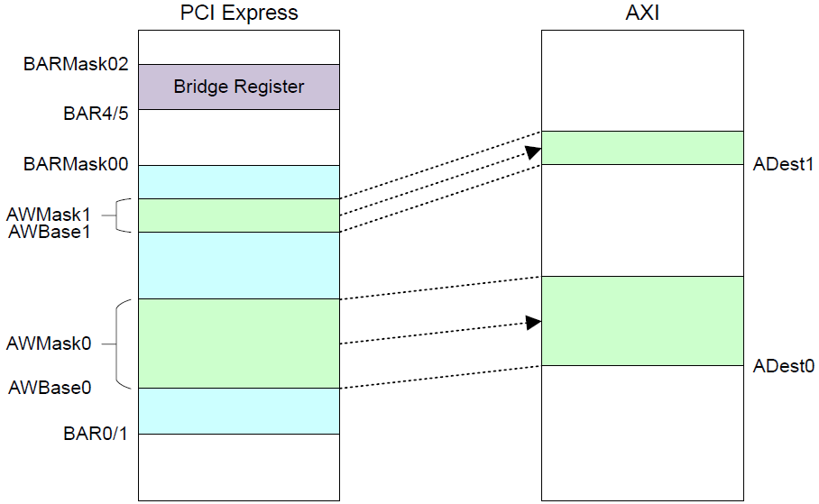
The AXI Window settings are used when MWr/MRd data from PCI Express is transferred to AXI bus (Data Receive operation via MWr/MRd request). Set AXI Window Base and AXI Window Mask in the BAR region. (BAR: PCI Express Configuration Register, Base Address Register)
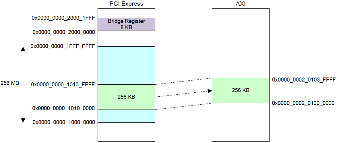
In Endpoint mode, bridge register is assigned to BAR4/5. Region size is 8 KB. BAR4/5 is 0x0000_0000_2000_0000 and BARMask02 is 0x0000_0000_0000_1FFFF (fixed). Consult Section "AXI Bridge Register" in the RZ microprocessor Hardware Manual for details.
Up to 4 AXI windows can be set by dividing the 64-bit memory space defined by each BAR. The mapping between BARs and AXI windows and the access addresses are as follows:
In the case of {BAR1, BAR0}, AXI Window 0, AXI Window 1, AXI Window 2 and AXI Window 3 can be used.
In the case of {BAR3, BAR2}, AXI Window 4, AXI Window 5, AXI Window 6 and AXI Window 7 can be used.
Up to four AXI windows can be configured in each BAR area. Setting examples of AXI windows allocated to each of the BAR areas is as follows:
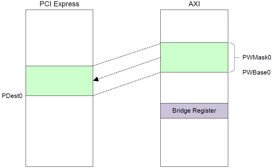
PCIe Window settings are used when MWr/MRd data from AXI bus is transferred to PCI Express (Data Transmit operation via MWr/MRd request). Access from the AXI side is converted into a PCIe request and then issued. A write transaction from the AXI via a window set as a PCIe window is converted into a MWr command and then issued. A read transaction from the AXI via a window set as a PCIe window is converted into an MRd command and then issued.
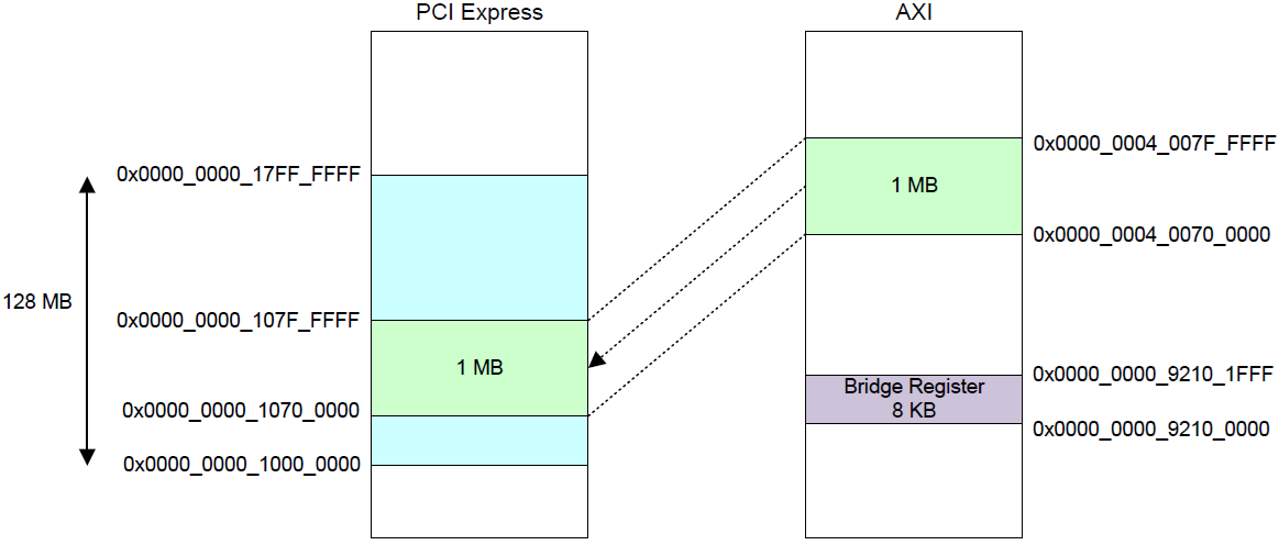
PCIe access address is shown as below.
Using the PCIE_EP HAL driver, other PCIe devices can be accessed through PCIEn space (8GB) or through PCIEn mirror space (256MB) (n=0,1). In particular, if the bus master supports 32-bit address space only, PCIEn space must be accessed through PCIEn mirror space. When using the mirror space, the address expander setting must first be configured in the BSP configuration. Consult Section "Address Expander" in the RZ microprocessor Hardware Manual for details.
Due to the characteristics of the Arm memory architecture, depending on the memory attributes, the order of access to peripherals memory space by the HAL driver and the access to the PCIEn memory space (including mirror area) by the user may not be guaranteed. In such cases, the user program must explicitly insert memory barrier instructions (such as __DMB() or __DSB()) after calling the HAL API function.
The below is an example of configuration space initialization.
This is a basic example of minimal use of the PCIE_EP module in an application.