|
RZT Flexible Software Package Documentation
Release v3.1.0
|
|
|
RZT Flexible Software Package Documentation
Release v3.1.0
|
|
Functions | |
| fsp_err_t | R_FSP_VersionGet (fsp_pack_version_t *const p_version) |
| void | Default_Handler (void) |
| BSP_TARGET_ARM BSP_ATTRIBUTE_STACKLESS void | system_init (void) |
| BSP_TARGET_ARM BSP_ATTRIBUTE_STACKLESS void | bsp_register_initialization (void) |
| void | SystemInit (void) |
| void | R_BSP_WarmStart (bsp_warm_start_event_t event) |
| BSP_ATTRIBUTE_STACKLESS void | R_BSP_WarmStart_StackLess (void) |
| void | R_BSP_CacheEnableInst (void) |
| void | R_BSP_CacheEnableData (void) |
| void | R_BSP_CacheEnableMemoryProtect (void) |
| void | R_BSP_CacheDisableInst (void) |
| void | R_BSP_CacheDisableData (void) |
| void | R_BSP_CacheDisableMemoryProtect (void) |
| void | R_BSP_CacheCleanAll (void) |
| void | R_BSP_CacheInvalidateAll (void) |
| void | R_BSP_CacheCleanInvalidateAll (void) |
| void | R_BSP_CacheCleanRange (uintptr_t base_address, uintptr_t length) |
| void | R_BSP_CacheInvalidateRange (uintptr_t base_address, uintptr_t length) |
| void | R_BSP_CacheCleanInvalidateRange (uintptr_t base_address, uintptr_t length) |
| void | R_BSP_CacheL3PowerCtrl (void) |
| __WEAK void | R_BSP_FspAssert (void) |
| __STATIC_INLINE IRQn_Type | R_FSP_CurrentIrqGet (void) |
| __STATIC_INLINE uint32_t | R_FSP_SystemClockHzGet (fsp_priv_clock_t clock) |
| void | R_BSP_SoftwareDelay (uint32_t delay, bsp_delay_units_t units) |
| __STATIC_INLINE void | R_FSP_IsrContextSet (IRQn_Type const irq, void *p_context) |
| Sets the ISR context associated with the requested IRQ. More... | |
| __STATIC_INLINE void | R_BSP_IrqClearPending (IRQn_Type irq) |
| __STATIC_INLINE uint32_t | R_BSP_IrqPendingGet (IRQn_Type irq) |
| __STATIC_INLINE void | R_BSP_IrqCfg (IRQn_Type const irq, uint32_t priority, void *p_context) |
| __STATIC_INLINE void | R_BSP_IrqEnableNoClear (IRQn_Type const irq) |
| __STATIC_INLINE void | R_BSP_IrqEnable (IRQn_Type const irq) |
| __STATIC_INLINE void | R_BSP_IrqDisable (IRQn_Type const irq) |
| __STATIC_INLINE void | R_BSP_IrqCfgEnable (IRQn_Type const irq, uint32_t priority, void *p_context) |
| __STATIC_INLINE void * | R_FSP_IsrContextGet (IRQn_Type const irq) |
| Finds the ISR context associated with the requested IRQ. More... | |
| __STATIC_INLINE void | R_BSP_IrqDetectTypeSet (IRQn_Type const irq, uint32_t detect_type) |
| __STATIC_INLINE void | R_BSP_IrqGroupSet (IRQn_Type const irq, uint32_t interrupt_group) |
| __STATIC_INLINE void | R_BSP_IrqMaskLevelSet (uint32_t mask_level) |
| __STATIC_INLINE uint32_t | R_BSP_IrqMaskLevelGet (void) |
| void | R_BSP_RegisterProtectEnable (bsp_reg_protect_t regs_to_protect) |
| void | R_BSP_RegisterProtectDisable (bsp_reg_protect_t regs_to_unprotect) |
| void | R_BSP_SystemReset (void) |
| void | R_BSP_CpuReset (bsp_reset_t cpu) |
| void | R_BSP_CpuResetAutoRelease (bsp_reset_t cpu) |
| void | R_BSP_CpuResetRelease (bsp_reset_t cpu) |
| void | R_BSP_ModuleResetEnable (bsp_module_reset_t module_to_enable) |
| void | R_BSP_ModuleResetDisable (bsp_module_reset_t module_to_disable) |
| BSP_TFU_INLINE float | __sinf (float angle) |
| BSP_TFU_INLINE float | __cosf (float angle) |
| BSP_TFU_INLINE void | __sincosf (float angle, float *sin, float *cos) |
| BSP_TFU_INLINE float | __atan2f (float y_cord, float x_cord) |
| BSP_TFU_INLINE float | __hypotf (float x_cord, float y_cord) |
| BSP_TFU_INLINE void | __atan2hypotf (float y_cord, float x_cord, float *atan2, float *hypot) |
| BSP_TFU_INLINE uint32_t | __sinfx (uint32_t angle) |
| BSP_TFU_INLINE uint32_t | __cosfx (uint32_t angle) |
| BSP_TFU_INLINE void | __sincosfx (uint32_t angle, uint32_t *sin, uint32_t *cos) |
| BSP_TFU_INLINE uint32_t | __atan2fx (uint32_t y_cord, uint32_t x_cord) |
| BSP_TFU_INLINE int32_t | __hypotfx (uint32_t x_cord, uint32_t y_cord) |
| BSP_TFU_INLINE void | __atan2hypotfx (uint32_t y_cord, uint32_t x_cord, uint32_t *atan2, int32_t *hypot) |
| BSP_ATTRIBUTE_STACKLESS void | r_bsp_software_delay_loop (__attribute__((unused)) uint32_t loop_cnt) |
| fsp_err_t | R_BSP_GroupIrqWrite (bsp_grp_irq_t irq, void(*p_callback)(bsp_grp_irq_t irq)) |
| void | R_BSP_GICD_SetCtlr (bsp_gicd_ctlr_bit_t bit) |
| uint32_t | R_BSP_GICD_GetCtlr (void) |
| void | R_BSP_GICD_Enable (bsp_gicd_ctlr_bit_t bit) |
| void | R_BSP_GICD_Disable (bsp_gicd_ctlr_bit_t bit) |
| void | R_BSP_GICD_AffinityRouteEnable (bsp_gicd_ctlr_bit_t bit) |
| void | R_BSP_GICD_SpiEnable (IRQn_Type irq) |
| void | R_BSP_GICD_SpiDisable (IRQn_Type irq) |
| void | R_BSP_GICD_SetSpiPriority (IRQn_Type irq, uint32_t priority) |
| uint32_t | R_BSP_GICD_GetSpiPriority (IRQn_Type irq) |
| void | R_BSP_GICD_SetSpiRoute (IRQn_Type id, uint64_t route, bsp_gicd_irouter_route_t mode) |
| uint64_t | R_BSP_GICD_GetSpiRoute (IRQn_Type id) |
| void | R_BSP_GICD_SetSpiSense (IRQn_Type irq, bsp_gicd_icfgr_sense_t sense) |
| uint32_t | R_BSP_GICD_GetSpiSense (IRQn_Type irq) |
| void | R_BSP_GICD_SetSpiPending (IRQn_Type irq) |
| uint32_t | R_BSP_GICD_GetSpiPending (IRQn_Type irq) |
| void | R_BSP_GICD_SetSpiClearPending (IRQn_Type irq) |
| uint32_t | R_BSP_GICD_GetSpiClearPending (IRQn_Type irq) |
| void | R_BSP_GICD_SetSpiSecurity (IRQn_Type irq, bsp_gic_igroupr_secure_t group) |
| void | R_BSP_GICD_SetSpiSecurityLine (uint32_t line, bsp_gic_igroupr_secure_t group) |
| void | R_BSP_GICD_SetSpiSecurityAll (bsp_gic_igroupr_secure_t group) |
| void | R_BSP_GICD_SetSpiClass (IRQn_Type id, bsp_gicd_iclar_class_t class_group) |
| void | R_BSP_GICR_Enable (void) |
| void | R_BSP_GICR_SgiPpiEnable (IRQn_Type irq) |
| void | R_BSP_GICR_SgiPpiDisable (IRQn_Type irq) |
| void | R_BSP_GICR_SetSgiPpiPriority (IRQn_Type irq, uint32_t priority) |
| uint32_t | R_BSP_GICR_GetSgiPpiPriority (IRQn_Type irq) |
| void | R_BSP_GICR_SetSgiPpiSense (IRQn_Type irq, bsp_gicd_icfgr_sense_t sense) |
| uint32_t | R_BSP_GICR_GetSgiPpiSense (IRQn_Type irq) |
| void | R_BSP_GICR_SetSgiPpiPending (IRQn_Type irq) |
| uint32_t | R_BSP_GICR_GetSgiPpiPending (IRQn_Type irq) |
| void | R_BSP_GICR_SetSgiPpiClearPending (IRQn_Type irq) |
| uint32_t | R_BSP_GICR_GetSgiPpiClearPending (IRQn_Type irq) |
| void | R_BSP_GICR_SetSgiPpiSecurity (IRQn_Type irq, bsp_gic_igroupr_secure_t group) |
| void | R_BSP_GICR_SetSgiPpiSecurityLine (bsp_gic_igroupr_secure_t group) |
| void | R_BSP_GICR_SetClass (bsp_gicd_iclar_class_t class_group) |
| uint32_t | R_BSP_GICR_GetRoute (void) |
| void | R_BSP_GICC_SetMaskLevel (uint64_t mask_level) |
| uint64_t | R_BSP_GICC_GetMaskLevel (void) |
| void | R_BSP_GICC_SetEoiGrp0 (IRQn_Type irq) |
| void | R_BSP_GICC_SetEoiGrp1 (IRQn_Type irq) |
| uint32_t | R_BSP_GICC_Get_IntIdGrp0 (void) |
| uint32_t | R_BSP_GICC_Get_IntIdGrp1 (void) |
| fsp_err_t | R_BSP_MmuVatoPa (uint64_t vaddress, uint64_t *p_paddress) |
| fsp_err_t | R_BSP_MmuPatoVa (uint64_t paddress, uint64_t *p_vaddress, bsp_mmu_conversion_flag_t cache_flag) |
| fsp_err_t | R_BSP_MemoryMap (r_mmu_pgtbl_cfg_t *p_memory_map_cfg) |
| fsp_err_t | R_BSP_MemoryUnMap (void) |
| fsp_err_t | R_BSP_MpuRegionDynamicConfig (bsp_mpu_dynamic_cfg_t *p_dynamic_region_cfg) |
| fsp_err_t | R_BSP_MpuRegionRestoreConfig (void) |
The BSP is responsible for getting the MCU from reset to the user's application. Before reaching the user's application, the BSP sets up the stacks, heap, clocks, interrupts, C runtime environment, and stack monitor.
Default initialization function.
All system clocks are set up during BSP initialization based on the settings in bsp_clock_cfg.h. These settings are derived from clock configuration information provided from the Configuration editor Clocks tab.
As Cortex-R ARM architecture, the Generic Interrupt Controller (GIC) handles exceptions and interrupt configuration, prioritization and interrupt masking. In the ARM architecture, the GIC handles IRQ and FIQ exceptions and receives the following interrupt types.
SGI and PPI are core-related specific interrupts, and SPI is connected to interrupts from each peripheral. GIC has interrupt number (INTID) internally. SGI uses INTID 0 to 15, PPI uses INTID 16 to 31, and SPI uses INTID 32 or later.
When multiplex interrupts are enabled, another interrupt can operated while one interrupt is operating.
If an interrupt occurs, it branches to BSP common handler and then to HAL interrupt handler. The user can choose whether to allow multiple interrupts in BSP common handler or in HAL interrupt handler.
There are two ways to enable it:
The behavior when multiplex interrupts are enabled in the BSP properties is as follows. Pink areas represent critical sections.
The behavior when multiplex interrupts are enabled for only HAL1 of the two HAL modules in the HAL module properties is as follows. Pink areas represent critical sections.
User configurable interrupts begin with slot 32 (SPI). These may be external, or peripheral generated interrupts.
The SPI is mapped along the Event Table, and the BSP allows the user to select only the events of interest as interrupt sources.
The weak attribute causes the declaration to be emitted as a weak symbol rather than a global. A weak symbol is one that can be overridden by an accompanying strong reference with the same name. When the BSP declares a function as weak, user code can define the same function and it will be used in place of the BSP function.
Weak symbols are supported for ELF targets and also for a.out targets when using the GNU assembler and linker.
Note that in CMSIS system.c, there is also a weak definition (and a function body) for the Warm Start callback function R_BSP_WarmStart(). Because this function is defined in the same file as the weak declaration, it will be called as the 'default' implementation. The function may be overridden by the user by copying the body into their user application and modifying it as necessary. The linker identifies this as the 'strong' reference and uses it.
As the BSP is in the process of bringing up the board out of reset, there are three points where the user can request a callback. These are defined as the 'Pre Clock Init', 'Post Clock Init' and 'Post C' warm start callbacks.
As described above, this function is already weakly defined as R_BSP_WarmStart(), so it is a simple matter of redefining the function or copying the existing body from CMSIS system.c into the application code to get a callback. R_BSP_WarmStart() takes an event parameter of type bsp_warm_start_event_t which describes the type of warm start callback being made.
This function is not enabled/disabled and is always called for both events as part of the BSP startup. Therefore it needs a function body, which will not be called if the user is overriding it. The function body is located in system.c. To use this function just copy this function into your own code and modify it to meet your needs. need to check
When an assertion or error occurs, the user assert function will be called.
This function is weakly defined as R_BSP_FspAssert(), so it is a simple matter of redefining the function or copying the existing body from bsp_common.c into the application code to manage assertions or errors.
If C Runtime is disabled, users must perform C runtime initialization themselves.
The BSP register protection functions utilize reference counters to ensure that an application which has specified a certain register and subsequently calls another function doesn't have its register protection settings inadvertently modified.
Each time R_BSP_RegisterProtectDisable() is called, the respective reference counter is incremented.
Each time R_BSP_RegisterProtectEnable() is called, the respective reference counter is decremented.
Both functions will only modify the protection state if their reference counter is zero.
Do not recommend using R_BSP_SoftwareDelay () for strict wait time processing. The reason we do not recommend using this API is that the Delay Time may change depending on the memory area where the execution program is placed.
Implements a blocking software delay. A delay can be specified in microseconds, milliseconds or seconds. The delay is implemented based on the system clock rate.
Implements Trigonometric math inline functions utilizing TFU hardware. These functions can calculate sine, cosine, arctangent and hypotenuse. The trigonometric library functions sinf(), cosf(), atan2f(), and hypotf() can be mapped to respective TFU functions by enabling TFU Mathlib property in FSP Configuration tool. Extended functions sincosf() and atan2hypotf() are also available when the TFU Mathlib property is enabled in the FSP Configuration editor.
TFU functions are not reentrant. Disable the TFU Mathlib property in Configuration editor if reentrant access to trigonometric library functions is required.
Implements a critical section. Interrupts with priority less than or equal to BSP_CFG_IRQ_MASK_LEVEL_FOR_CRITICAL_SECTION are not serviced in critical sections. Interrupts with higher priority than BSP_CFG_IRQ_MASK_LEVEL_FOR_CRITICAL_SECTION still execute in critical sections.
Variables placed in the following sections will be invalidated for caching.
To place the variables in these noncache sections, use the BSP_PLACE_IN_SECTION macro to define them. (e.g. uint32_t value BSP_PLACE_IN_SECTION(".data_noncache") = 1)
Data with and without initial values can be placed.
FSPv3.0 or later, the memory layout will be changed as follows:
Attributes and Regions can be set in the CPU-MPU/MMU of the BSP property.
For example, in the SystemRAM area, the cacheability settings shown below are used:
The configuration values are generated as macro values in bsp_mcu_cpu_memory_cfg.h and are reflected in the ARM core registers in the startup code.
In the CPU-MPU configuration, it is feasible to configure memory attributes tailored to specific applications. For instance, the Normal memory attribute facilitates high-speed access, rendering it suitable for RAM access and instruction execution. Conversely, the Device memory attribute enforces strict execution order, making it apt for peripheral register access and flash memory write operations.
Moreover, the system is capable of detecting and reporting faults in the event of unforeseen access to each memory attribute.
A comprehensive understanding of these specifications is crucial in preventing improper memory access and unintended aborts. Below are some examples of how each memory attribute can be utilized. For detailed information, please consult the Technical Reference Manual and Architecture Reference Manual published by ARM.
Glossary of key terms used in this document:
In addition to configuring MPU regions via BSP properties in the BSP tab, run-time configuration is also supported, offering greater flexibility. Please use the following BSP API function for configuring a dynamic region and reset the setting to initial value:
R_BSP_MpuRegionDynamicConfig () has been executed, it cannot run again until R_BSP_MpuRegionRestoreConfig () is performed.Configure dynamic region in the bsp_mpu_dynamic_cfg_t in the following file.
{rz device}/fsp/src/bsp/mcu/all/cr/bsp_mpu_core.h
The configuration structure is show as below.
base address
Set the base address of the dynamic region. The address must be aligned with 64 bytes.
size
Set the size of the dynamic region. The input size is not less than 64 bytes and must increase in increments of 64 bytes.
attribute
Configures the attribute properties of the dynamic region. All required properties must be specified by the user.
These setting value by using a macro of Access Permission, Shareability, Attribute Index and Other.
Access Permision macro
| Name | Description |
|---|---|
| BSP_EL1RW_EL0NO | Privileged mode: read/write possible, user mode: not accessible |
| BSP_EL1RW_EL0RW | Privileged mode: read/write possible, user mode: read/write possible |
| BSP_EL1RO_EL0NO | Privileged mode: read only , user mode: not accessible |
| BSP_EL1RO_EL0RO | Privileged mode: read only , user mode: read only |
Shareability macro
| Name | Description |
|---|---|
| BSP_NON_SHAREABLE | A domain limited to the local agent and do not require synchronization with other cores, processors, or devices. |
| BSP_INNER_SHAREABLE | A domain that is shared by other agents, but not necessarily all agent in the system. |
| BSP_OUTER_SHAREABLE | A domain that is shared by multiple agents that can consist of one or more Inner Shareable domains. |
Attribute Index maco
| Name | Description |
|---|---|
| BSP_ATTRINDEX0 | Attribute Index 0. |
| BSP_ATTRINDEX1 | Attribute Index 1. |
| BSP_ATTRINDEX2 | Attribute Index 2. |
| BSP_ATTRINDEX3 | Attribute Index 3. |
| BSP_ATTRINDEX4 | Attribute Index 4. |
| BSP_ATTRINDEX5 | Attribute Index 5. |
| BSP_ATTRINDEX6 | Attribute Index 6. |
| BSP_ATTRINDEX7 | Attribute Index 7. |
Regarding the memory attribute properties such as Memory type and Inner/Outer Attribute settings, these will be set up in CPU MPU|Attribute property in FSP Configuration tool.
Other macro
| Name | Description |
|---|---|
| BSP_EXECUTE_ENABLE | Programs will be allowed to run in the region. |
| BSP_EXECUTE_NEVER | programs will be prohibited from running in the region. |
Example of dynamically region allocated
The following pattern illustrates how a 128-byte region is dynamaically allocated.
In the CPU-MMU (CA55), a virtual address is assigned to a physical address, so the CPU accesses the virtual address. The use of virtual addresses enables access with different attributes from the CPU. For example, in RZ/T2H CA55, a virtual address noncache is placed in the area offset 0x0020_0000 (Reserved) from the physical address (System SRAM) in order to realize cache access to System SRAM and access noncache.
Note that if a bus master other than the CPU accesses the same resource, direct access to the physical address is required. For example, when setting the source/destination address for a DMA transfer, the virtual address must be converted to a physical address. If address translation is required within a driver, such as FSP's DMAC driver, the BSP APIs (R_BSP_MmuVatoPa, R_BSP_MmuPatoVa) are used to perform address translation. If address translation is required within a user application, these BSP APIs should be used. Refer to FSP Module (DMAC, USB, Ethernet) for specific implementation examples of BSP API.
The CPU-MMU assigns two virtual addresses with different cache attributes to a single physical region to enable both cached memory access and non-cached DMA access to a shared memory region.
When using this CPU-MMU configuration, it is essential to maintain data consistency, processing order, and coherency. When accessing the target memory regions from a user application, ensure that cache cleaning and invalidation, as well as DMB barrier instructions, are executed to guarantee shared access. For more information, refer to the Arm Architecture Reference Manual.
Glossary of key terms used in this document:
In addition to configuring MMU regions via BSP properties in the BSP tab, run-time configuration is also supported, offering greater flexibility. Please use the following BSP API function for configuring a dynamic region and reset the setting to initial value:
R_BSP_MemoryMap () has been executed, it cannot run again until R_BSP_MemoryUnMap () is performed.Configure dynamic region in the r_mmu_pgtbl_cfg_t in the following file.
{rz device}/fsp/src/bsp/mcu/all/ca/bsp_mmu_core.h
The configuration structure is show as below.
Virtual address
Set the virtual address of the dynamic area. If the address is less than 4GB area, it must be aligned with 2M-bytes, and if it is more than 4GB area, it must be aligned with 1G-bytes.
Physical address
Set the physical address of the dynamic area. If the virtual address is less than 4GB, it must be aligned to 2MB. Also, the virtual address and bit21-bit0 must match.If the virtual address exceeds 4GB, it must be aligned to 1GB. Also, the virtual address and bit30-bit0 must match.
Size
Set the size of the dynamic region. If the virtual address is less than 4GB area, it must be aligned with 2M-bytes, and if it is more than 4GB area, it must be aligned with 1G-bytes.
Attribute
Configures the attribute properties of the dynamic memory mapping. All required properties must be specified by the user.
These setting value by using a macro of Access Permission, Shareability, Attribute Index and Other.
Unprivileged Execute Never (UXN) macro
| Name | Description |
|---|---|
| BSP_UXN_EXECUTE_ENABLE | Can be executed in unprivileged mode |
| BSP_UXN_EXECUTE_DISABLE | Cannot run in unprivileged mode |
Privileged Execute Never (PXN) macro
| Name | Description |
|---|---|
| BSP_PXN_EXECUTE_ENABLE | Can be executed in privileged mode |
| BSP_PXN_EXECUTE_DISABLE | Cannot run in privileged mode |
Shareability macro
| Name | Description |
|---|---|
| BSP_NON_SHAREABLE | A domain limited to the local agent and do not require synchronization with other cores, processors, or devices |
| BSP_INNER_SHAREABLE | A domain that is shared by other agents, but not necessarily all agent in the system |
| BSP_OUTER_SHAREABLE | A domain that is shared by multiple agents that can consist of one or more Inner Shareable domains |
Access Permision macro
| Name | Description |
|---|---|
| BSP_EL321RW_EL0NO | Unprivileged mode(EL1,EL2,EL3): read/write possible, Privileged mode(EL0): not accessible |
| BSP_EL321RW_EL0RW | Unprivileged mode(EL1,EL2,EL3): read/write possible, Privileged mode(EL0): read/write possible |
| BSP_EL321RO_EL0NO | Unprivileged mode(EL1,EL2,EL3): read only, Privileged mode(EL0): not accessible |
| BSP_EL321RO_EL0RO | Unprivileged mode(EL1,EL2,EL3): read only, Privileged mode(EL0): read only |
Attribute Index macro
| Name | Description |
|---|---|
| BSP_ATTRINDEX0 | Attribute Index 0 |
| BSP_ATTRINDEX1 | Attribute Index 1 |
| BSP_ATTRINDEX2 | Attribute Index 2 |
| BSP_ATTRINDEX3 | Attribute Index 3 |
| BSP_ATTRINDEX4 | Attribute Index 4 |
| BSP_ATTRINDEX5 | Attribute Index 5 |
| BSP_ATTRINDEX6 | Attribute Index 6 |
| BSP_ATTRINDEX7 | Attribute Index 7 |
Regarding the memory attribute properties such as Memory type and Inner/Outer Attribute settings, these will be set up in CPU MMU|Attribute property in FSP Configuration tool.
Security bit(only EL3 and EL1)
| Name | Description |
|---|---|
| BSP_NS_SECURE | Secure |
| BSP_NS_NON_SECURE | Non Secure |
Other macro
| Name | Description |
|---|---|
| BSP_REGION_ENABLE | Enable the region of the specified virtual address |
| BSP_REGION_DISABLE | Disable the region of the specified virtual address |
Example of dynamically region allocated
The following pattern illustrates how a 2M-byte region is dynamaically allocated.
The TZC-400 module can be configured from the BSP properties of the RZ microprocessor containing the TZC-400.
The configuration values are generated as macro values in bsp_mcu_tzc400_memory_cfg.h and reflected in the ARM core registers in the startup code.
The default settings of the TZC-400 modules allow access in unprivileged and privileged in non-secure and secure in region 0.
For example, in RZT2H device, when creating the access rule in TZC-400-0: DDR SDRAM A0/A1 I/F, the settings shown below are used:
The BSP shall provide a method to enable or cancel module stop for a given peripheral channel.
The reset state and the release can be set for each peripheral module. To secure processing after release from a module reset, dummy read the same register at sevral times after writing to initiate release from the module reset.
When a request signal is input to the SEI pin (or NMI pin), a System Error Interrupt occurs. The sequence to detect a System Error Interrupt is different for each core.
Cortex-R52
The SEI pin is connected to SEI and VSEI in Cortex-R52 CPU0 and CPU1, and an asynchronous external abort occurs when a request signal is input.
The implementation method is described below.
Here is how the implementation example works.
Cortex-A55
The SEI pin is connected to Shared Peripheral Interrupt(SPI), and a SPI occurs when a request signal is input. It is possible to detect SEI by interrupt generation due to the event number of SPI.
The implementation method is described below.
Here is how the implementation example works.
The FSP applies the DDR parameter file generated by the DDR parameter generation tool (hereinafter referred to as "gen_tool"). The procedure for modifying the DDR parameter file is as follows.
Let's assume the file name of the file generated by gen_tool is "param_ddrinit_ref_lpddr4_r02p03.h".
To prevent build warnings, the GCC linker script separates the placement regions for .text and .data. (The same goes for .loader_text and .loader_data)
Below is a simplified version of fsp_ram_execution.ld.
.text is placed in RAM_TEXT, and .data is placed in RAM_DATA. The start address and size of both regions are the same.
Also, the start address of .data is set to the end address of .ARM.exidx. Without this, .data would be placed at the beginning of RAM_DATA and would overlap with .text.
For example, if you want to move .ARM.exidx to the BTCM region, modify the end address of .ARM.extab to match the start address of .data.
You can change the program placement region by configuring the settings described below.
This only applies to Cortex-R52, which has a TCM implemented.
Therefore, it does not apply to the Cortex-R52 CPU1 of RZ/T2M and RZ/T2ME.
Change the location region for the following two types of programs:
The placement region that can be changed are as follows:
The symbols "LOADER_PROGRAM_LOCATION_PRV" and "USER_PROGRAM_LOCATION_PRV" are defined in the linker script, and the location is changed depending on these values.
The values correspond to the following locations:
The setting method varies depending on the IDE.
e² studio The following additional properties must be set.
EWARM The following additional properties must be set.
When operating in multi-core, the primary and secondary core copy code and data from ROM to RAM.
Changing the pins accessed by the ROM boot during this copy process can cause it to fail. Specifically, changing the ROM boot pins in the primary's Pins tab may lead to this issue.
To work around this, the Pins tab preserves the ROM boot pin settings. Instead, configure the pins using the IOPORT driver's API on the user application side after each core's startup is complete.
In eSD boot mode (if the device supports), device boots a program from an external eSD device (including SD card) with 4-bit data bus. In FSP, you can create a write image file for the SD card by building a project for eSD boot mode. The created image file can be written to the SD card using a tool on your PC.
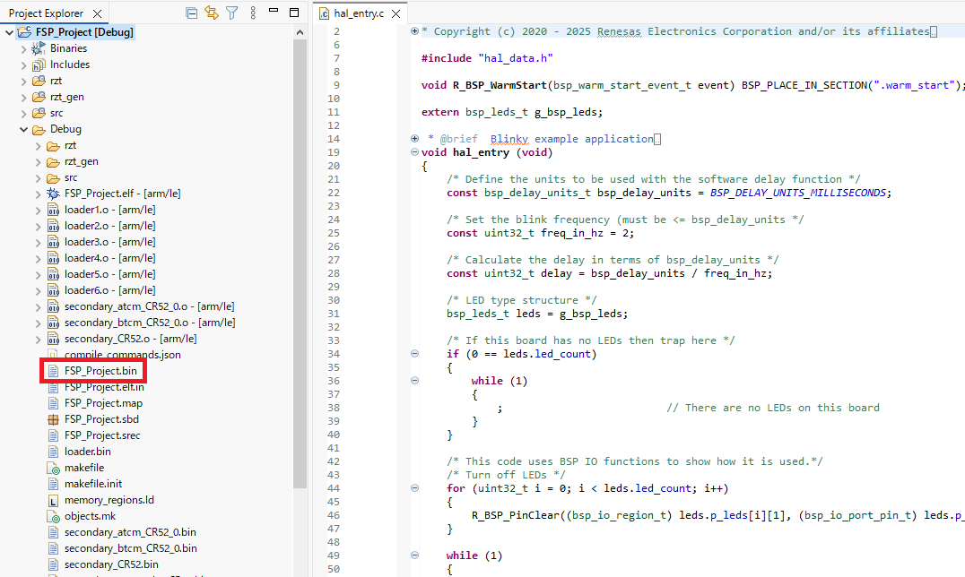
LOADER_PROGRAM_SIZE = 0x8000; .Therefore, if LDR_SIZE_NML is changed from its default value in the FSP Configurator, the value of LOADER_PROGRAM_SIZE in the linker file must also be modified to match.When using e² studio, after building the project, the <project_name>.bin file is created in the Debug folder as a write image file for the SD card. Use the SD card writing tool on your PC to write the created image file to the SD card.
To perform multiplexing of the loader program, follow the procedure below. Skip the procedure if multiplexing is not required. Note that loader parameters are multiplexed by default. Refer to "Allocation of the Loader Parameter and Loader Program" in the RZ microprocessor User's Manual for details.
When the project is built, loader1.o - loader6.o are also generated in the Debug folder. To include loader1.o - loader6.o at subsequent builds, set loader1.o - loader6.o in the Other objects section of e² studio's Linker settings. This allows to place the loader program in spare areas #1-#6. To prevent build errors, this configuration must be set after loader1.o - loader6.o are generated in a prior build.
Following additional properties must be set.
Set file path of loader1.o - loader6.o files in the project to Other objects
${workspace_loc:/${ProjName}/Debug/loader1.o}
${workspace_loc:/${ProjName}/Debug/loader2.o}
${workspace_loc:/${ProjName}/Debug/loader3.o}
${workspace_loc:/${ProjName}/Debug/loader4.o}
${workspace_loc:/${ProjName}/Debug/loader5.o}
${workspace_loc:/${ProjName}/Debug/loader6.o}

When the project is built again, loader1.o -loader6.o are linked, and an image file with a multiplexed loader program is generated in the Debug folder. It can be written to the SD card.
When using EWARM, set the Output format of the Output Converter to "Raw binary".
Following additional properties must be set.
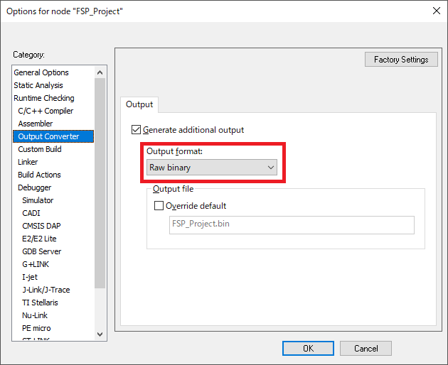
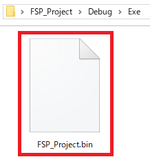
This allows to create a <project_name>.bin file in the Debug/Exe folder as a write image file for the SD card. Use the SD card writing tool on your PC to write the created image file to the SD card.
To perform multiplexing of the loader program, follow the procedure below. Skip the procedure if multiplexing is not required. Note that loader parameters are multiplexed by default. Refer to "Allocation of the Loader Parameter and Loader Program" in the RZ microprocessor User's Manual for details.
To place the loader program in spare areas #1 to #6, extract the loader program.
Following additional properties must be set.
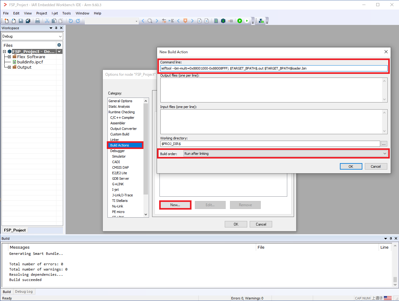
a. Command line
ielftool --bin-multi=0x88001000-0x88008FFF; $TARGET_BPATH$.out $TARGET_BPATH$loader.bin
b. Build order
Set "Run after Linking" for the Build order.
When the project is built, <project_name>loader-0x88001000.bin is generated in the Debug/Exe folder as a binary for placing in spare areas #1 to #6.
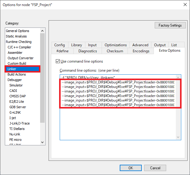
To import .bin file at subsequent builds and place it in the spare areas #1 to #6, add the image_input definition LOADER1 - LOADER6 to Linker > Extra Options and keep LOADER1 - LOADER6 symbols at Linker > Input > Keep symbols
Following additional properties must be set.
Click Linker > Extra Options and add as follows:
--image_input=$PROJ_DIR$\Debug\Exe\<project_name>loader-0x88001000.bin,LOADER1,LOADER1,8
--image_input=$PROJ_DIR$\Debug\Exe\<project_name>loader-0x88001000.bin,LOADER2,LOADER2,8
--image_input=$PROJ_DIR$\Debug\Exe\<project_name>loader-0x88001000.bin,LOADER3,LOADER3,8
--image_input=$PROJ_DIR$\Debug\Exe\<project_name>loader-0x88001000.bin,LOADER4,LOADER4,8
--image_input=$PROJ_DIR$\Debug\Exe\<project_name>loader-0x88001000.bin,LOADER5,LOADER5,8
--image_input=$PROJ_DIR$\Debug\Exe\<project_name>loader-0x88001000.bin,LOADER6,LOADER6,8
Click Linker > Input and set it as follows:
Keep symbols (one per line).
LOADER1
LOADER2
LOADER3
LOADER4
LOADER5
LOADER6
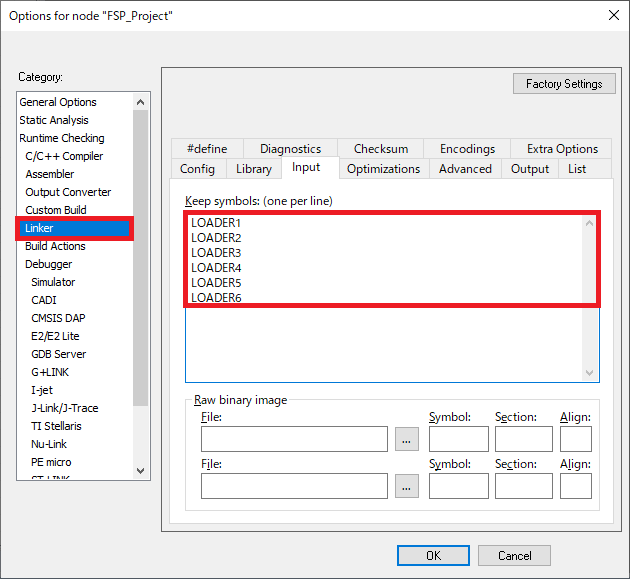
When the project is built again, <project_name>loader-0x88001000.bin is linked, and an image file with a multiplexed loader program is generated in the Debug/Exe folder. It can be written to the SD card.
Using an SD card writing tool on your PC, write the created image file to the SD card. Use a tool similar to the following:
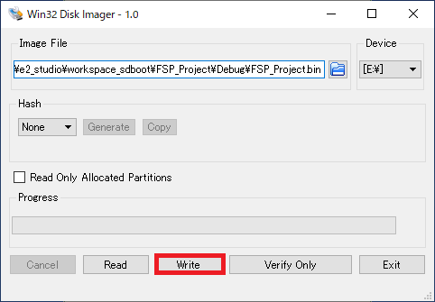
This section shows how to write to an SD card using PC tool Win32 Disk Imager for example. The binary data of the image file is written starting from the first sector of the SD card.
Select the generated SD card image file <project_name>.bin as the write image file. When selecting the file, set "*.*" to enable selection of .bin files.

Click Write to write the image file to the SD card.
Set the eSD boot mode using the MD pins of the device. Insert the SD card into the SD card slot connected to the device, then turn the power ON. Device boots a program from the SD card.
Insert the loop part in startup_core.c according to "Appendix. How to Debug FSP Project with Flash Boot Mode" in RZ/T2, RZ/N2 Getting Started with Flexible Software Package.
The eSD boot project can be debugged as the flash boot project described in RZ/T2, RZ/N2 Getting Started with Flexible Software Package. However, the following settings are different for eSD boot project debugging:
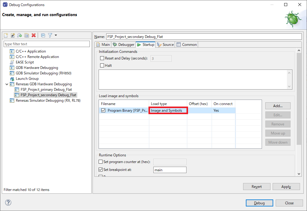
For primary project, change the Load type in the e² studio debugger connection settings from "Image and Symbols" to "Symbols only".
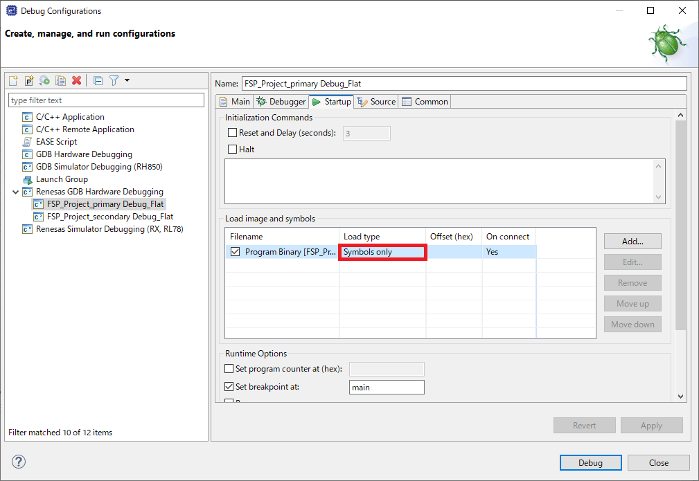
For secondary (or later) project, leave the Load type as "Image and Symbols" in the e² studio debugger connection settings. No change is necessary.
The eSD boot project can be debugged as the flash boot project described in RZ/T2, RZ/N2 Getting Started with Flexible Software Package. However, establish a debug connection while the program is running.
The SD card written with image file created by the FSP Project contain a valid MBR (Master Boot Record) area in the first sector. However, no partition table has been created. By creating a FAT partition using a disk management tool, the FSP program and the FAT file system can coexist on the SD card.
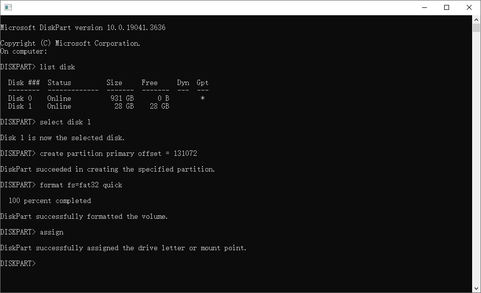
For example, using the DISKPART tool provided as standard on Windows PCs, a FAT partition is created as follows.
Insert the SD card written with image file created by the FSP Project into your PC. Launch the DISKPART tool on your Windows PC and execute the following command. This create a FAT partition on the SD card. When creating a FAT partition, it is recommended to add an offset of certain bytes from the beginning of the SD card to avoid overlapping with the pre-written FSP program.
The following is an example of creating a FAT partition by adding an offset of 128MB (=131072KB) from the beginning of the SD card.
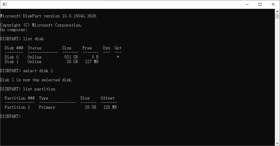
You can check the partitions on the SD card.
The following is an example of confirming that a FAT partition has been created with an offset of 128MB (=131072KB) from the beginning of the SD card.
select disk n. "n" depends on the development environment. If selected a different disk and issue the partition management command, the disk may become unusable.In eMMC boot mode (if the device supports), device boots a program from an external eMMC device with 8-bit data bus. In FSP, you can create a write image file for the eMMC by building a project for eMMC boot mode. The created image file can be written to the eMMC using a tool on your PC.
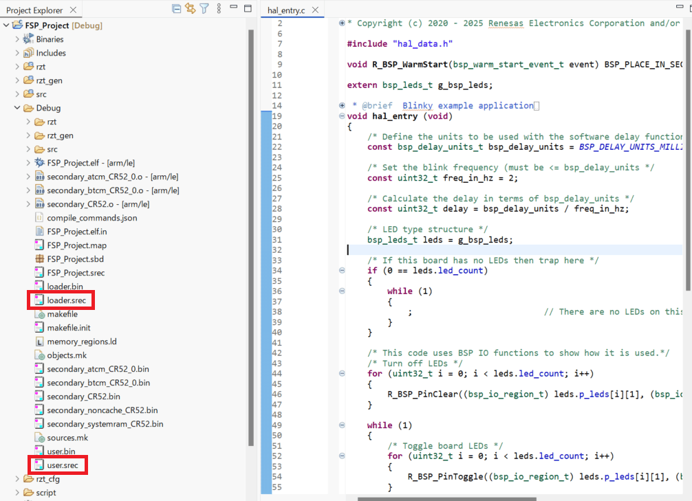
LOADER_PROGRAM_SIZE = 0x8000; .Therefore, if LDR_SIZE_NML is changed from its default value in the FSP Configurator, the value of LOADER_PROGRAM_SIZE in the linker file must also be modified to match.When using e² studio, after building the project, the loader.srec and user.srec file is created in the Debug folder as a write image file for the eMMC. Use the eMMC writing tool on your PC to write the created image file to the eMMC.
Use a Motorola S-record conversion tool to split the image file into .srec files for the loader parameters/loader program and the user application. Use a tool similar to the following;
This section demonstrates how to split the file using, for example, the PC tool SRecord.
The following instructions assume that the SRecord executable directory has been added to the Windows PC PATH environment variable. Example: C:\Program Files\srecord\bin
Following additional properties must be set in EWARM.
1.Click Project > Options... 2.Click Build Actions > Build Actions Configuration > New and set it as follows:
| No. | Command line: | Output files | Input files | Working directory | Build order |
|---|---|---|---|---|---|
| 1 | srec_cat $TARGET_BPATH$.srec -crop 0x88000000 0x88008FFF -offset -0x88000000 -o $PROJ_DIR$\Debug\Exe\loader.srec -motorola -address-length=4 -Output_Block_Size 16 -execution-start-address=0 | loader.srec | $TARGET_BPATH$.srec | $PROJ_DIR$ | Run after linking |
| 2 | srec_cat $TARGET_BPATH$.srec -crop 0x88009000 0x93FFFFFF -offset -0x88009000 -o $PROJ_DIR$\Debug\Exe\user.srec -motorola -address-length=4 -Output_Block_Size 16 -execution-start-address=0 | user.srec | $TARGET_BPATH$.srec | $PROJ_DIR$ | Run after linking |
3.When the project is built, loader.srec and user.srec are generated in the Debug/Exe folder.

Using an eMMC writing tool on your PC, write the created image file to the eMMC. Use a tool similar to the following;
This section shows how to write to an eMMC using PC tool Linux Flash Programmer for example. The binary data of the image file is written starting from the first sector of the eMMC.
Execute SCI boot and download the Linux Flash Programmer to the RAM of the RZ microprocessor.
1.Connect between the board and a control PC by USB serial cable.
2.Launch the terminal software and specify the serial port of board.
3.Select the Setup > Serial port to set the settings about serial communication protocol on the software. Set the settings about serial communication protocol on a terminal software as below:
4.Configure the SCI boot mode using the MD pins of the device.
5.After finishing all settings, turn on power, the messages below are displayed on the terminal.
6.Below is a sample procedure with Tera Term. Drag HDR NM file and drop the file to the Tera Term window, then click OK.
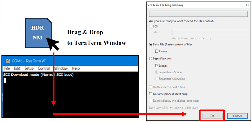
7.The image will be sent to the board via serial connection. After completing that, send Flash_Programmer_SCIF_CR52_RZT2H_EVK.mot as same as HDR NM. Send it as soon as possible.
8.After successfully downloading the binary, Flash Programmer starts automatically and shows a message like below on the terminal.
Next, write two image files to the eMMC.
Follow the steps below to operate Tera Term.
9.Execute the EMMCWECSD command with the arguments 0xb3 0x9 to enable access to the eMMC boot partition 1.
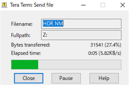
10.Execute the EMMCW command with arguments 0x0 0x0. When "send file" is displayed, drag loader.srec file and drop the file to the Tera Term window, then click “OK”. When the transfer is complete, "EMMCW Complete!" will be displayed.
11.Execute the EMMCWECSD command with the arguments 0xb3 0x8 to enable access to the user area.
12.Execute the EMMCW command with arguments 0x0 0x0. When "send file" is displayed, drag user.srec file and drop the file to the Tera Term window, then click “OK”. When the transfer is complete, "EMMCW Complete!" will be displayed.
13.Execute the EMMCWECSD command with the arguments 0xb1 0x2 to change the eMMC boot access bus width to 8-bit.
14.After writing loader.srec and user.srec files normally, turn off the power switch of the board.
15.Configure the eMMC boot mode using the MD pins of the device. Then turn the power ON. Device boots a program from the eMMC.
The debugging procedure is the same as eSD boot. Refer to the How to debug an eSD boot project section in this document.
Exclusive access instructions for synchronization and semaphores in Cortex-R52 and Cortex-A55 are prohibited to System SRAM. For exclusive control, perform either of the below methods,
For details of the target instructions, see the below sections in Arm Architecture Reference Manual for A-profile architecture (DDI 0487).
The BSP is heavily data driven with most features and functionality being configured based on the content from configuration files. Configuration files represent the settings specified by the user and are generated when the project is built and/or when the Generate Project Content button is clicked in the FSP Configuration editor.
| Configuration | Options | Default | Description |
|---|---|---|---|
| MCU Vcc (mV) | Value must between 0 and 3800 (3.8V) | 3300 | Some peripherals require different settings based on the supplied voltage. Entering Vcc here (in mV) allows the relevant driver modules to configure the associated peripherals accordingly. |
| Parameter checking |
| Disabled | When enabled, parameter checking for the BSP is turned on. In addition, any modules whose parameter checking configuration is set to 'Default (BSP)' will perform parameter checking as well. |
| Assert Failures |
| Return FSP_ERR_ASSERTION | Define the behavior of the FSP_ASSERT() macro. |
| Error Log |
| No Error Log | Specify error logging behavior. |
| Soft Reset |
| Disabled | Support for soft reset. If disabled, registers are assumed to be set to their default value during startup. |
| Port Protect |
| Enabled | Keep the write protection function related GPIO settings locked when they are not being modified. If disabled they will be unlocked during startup. |
| Early BSP Initialization |
| Disabled | Enable this option to use BSP functions before C runtime initialization (BSP_WARM_START_RESET or BSP_WARM_START_POST_CLOCK). |
| Multiplex Interrupt |
| Disabled | Enable multiplex interrupt system-wide. |
| Register Protect Polling Count | Value must between 0x1 and 0xFFFFFFFF | 0xFFFFFFFF | When the semaphore is enabled, the semaphore is acquired in order to configure the protect register. While waiting for the semaphore to become available, the protect register is polled the number of times indicated by this counter. |
In the case of the secondary project (Non-primary cores), duplicate resource are indicated as the followings in Configuration tab when using resources that are used in the linked the primary (CR52_0 (CPU0) or CA55_0) project.
RZ/T2 uses Cortex-R52(CR52) and Cortex-A55(CA55) cores. The following is a cautionary execution when porting programs to different cores.
| Specifications | CR52 | CA55 | Porting from CR52 to CA55 | Porting from CA55 to CR52 |
|---|---|---|---|---|
| Instruction set | AArch32 (32bit) | AArch64 (64bit) | Stack consumption doubles as CPU registers go from 32-bit to 64-bit. | - |
| Address space | 4GB | 32GB | Pointer type size changes from 32-bit to 64-bit. | Data placed in areas larger than 4 GB will need to be rearranged. |
| Cache | Instruction/data cache | L1 instruction/data cache L2 cache L3 cache | - | CA55-specific BSP API cannot be used. - R_BSP_CacheL3PowerCtrl() |
| Memory management | CPU-MPU | CPU-MMU | The non-cache section placed in System SRAM is allocated to a different area (Reserved) from the physical address as a virtual address. When handling physical addresses in user applications, address conversion is performed using the BSP API (R_BSP_MmuVatoPa, R_BSP_MmuPatoVa) that converts addresses. | CA55-specific BSP API cannot be used. - R_BSP_MmuVatoPa() - R_BSP_MmuPatoVa() |
| Interrupt | GIC | GIC-600 | - | CA55-specific BSP API cannot be used. - R_BSP_GICD_xxxx() - R_BSP_GICR_xxxx() - R_BSP_GICC_xxxx() |
| Trigonometric Function Unit (TFU) | FSP supported | FSP not supported | Unable to use TFU-related BSP API. | - |
| System Error Interrupt (SEI,NMI) | Asynchronous external abort | SPI | Please refer to the implementation guide in the System Error Interrupt (SEI,NMI) section. | Refer to the left |
Modules | |
| RZT2H | |
| RZT2L | |
| RZT2M | |
| RZT2ME | |
Macros | |
| #define | BSP_IRQ_DISABLED |
| #define | FSP_RETURN(err) |
| #define | FSP_ERROR_LOG(err) |
| #define | FSP_ASSERT(a) |
| #define | FSP_ASSERT_NOT_RETURN_VALUE(a) |
| #define | FSP_ERROR_RETURN(a, err) |
| #define | FSP_ERROR_NOT_RETURN_VALUE(a, err) |
| #define | FSP_CRITICAL_SECTION_ENTER |
| #define | FSP_CRITICAL_SECTION_EXIT |
| #define | FSP_INVALID_VECTOR |
| #define | BSP_CFG_HANDLE_UNRECOVERABLE_ERROR(x) |
| #define | BSP_SECTION_AARCH64_STACK |
| #define | BSP_STACK_ALIGNMENT |
| #define | R_BSP_MODULE_START(ip, channel) |
| #define | R_BSP_MODULE_STOP(ip, channel) |
Enumerations | |
| enum | fsp_ip_t |
| enum | fsp_signal_t |
| enum | bsp_warm_start_event_t |
| enum | bsp_delay_units_t |
| enum | bsp_reg_protect_t |
| enum | bsp_reset_t |
| enum | bsp_cluster_reset_auto_release_t |
| enum | bsp_module_reset_t |
| enum | bsp_resource_state_t |
| enum | bsp_resource_num_t |
| enum | bsp_grp_irq_t |
Variables | |
| uint32_t | SystemCoreClock |
| #define BSP_IRQ_DISABLED |
Used to signify that an ELC event is not able to be used as an interrupt.
| #define FSP_RETURN | ( | err | ) |
Macro to log and return error without an assertion.
| #define FSP_ERROR_LOG | ( | err | ) |
This function is called before returning an error code. To stop on a runtime error, define fsp_error_log in user code and do required debugging (breakpoints, stack dump, etc) in this function.
| #define FSP_ASSERT | ( | a | ) |
Default assertion calls FSP_ERROR_RETURN if condition "a" is false. Used to identify incorrect use of API's in FSP functions.
| #define FSP_ASSERT_NOT_RETURN_VALUE | ( | a | ) |
Default assertion calls FSP_ERROR_NOT_RETURN_VALUE if condition "a" is false. Used to identify incorrect use of API's in FSP functions.
| #define FSP_ERROR_RETURN | ( | a, | |
| err | |||
| ) |
All FSP error codes are returned using this macro. Calls FSP_ERROR_LOG function if condition "a" is false. Used to identify runtime errors in FSP functions.
| #define FSP_ERROR_NOT_RETURN_VALUE | ( | a, | |
| err | |||
| ) |
This function performs the same operation as FSP_ERROR_RETURN, but can be applied to functions that do not return an error code.
| #define FSP_CRITICAL_SECTION_ENTER |
This macro temporarily saves the current interrupt state and disables interrupts.
| #define FSP_CRITICAL_SECTION_EXIT |
This macro restores the previously saved interrupt state, reenabling interrupts.
| #define FSP_INVALID_VECTOR |
Used to signify that the requested IRQ vector is not defined in this system.
| #define BSP_CFG_HANDLE_UNRECOVERABLE_ERROR | ( | x | ) |
In the event of an unrecoverable error, the BSP will by default take no action. The user can override this default behavior by defining their own BSP_CFG_HANDLE_UNRECOVERABLE_ERROR macro.
When BSP_CFG_HANDLE_UNRECOVERABLE_ERROR is called from error handlers, the user will need to investigate the cause. Common problems are stack corruption or the use of an invalid pointer.
Use the Fault Status window in e2 studio or manually check the fault status registers for more information. After an error handler, other interrupts may occur. Therefore, override BSP_CFG_HANDLE_UNRECOVERABLE_ERROR macro with a user-defined function and place a breakpoint inside it. This will help you catch the first interrupt and identify the root cause of the error.
| #define BSP_SECTION_AARCH64_STACK |
Common macro for FSP header files. There is also a corresponding FSP_FOOTER macro at the end of this file.
| #define BSP_STACK_ALIGNMENT |
Stacks (and heap) must be sized and aligned to an integer multiple of this number.
| #define R_BSP_MODULE_START | ( | ip, | |
| channel | |||
| ) |
Cancels the module stop state.
| ip | fsp_ip_t enum value for the module to be stopped |
| channel | The channel. Use channel 0 for modules without channels. |
| #define R_BSP_MODULE_STOP | ( | ip, | |
| channel | |||
| ) |
Enables the module stop state.
| ip | fsp_ip_t enum value for the module to be stopped |
| channel | The channel. Use channel 0 for modules without channels. |
| enum fsp_ip_t |
Available modules.
| enum fsp_signal_t |
Signals that can be mapped to an interrupt.
Different warm start entry locations in the BSP.
| enum bsp_delay_units_t |
Available delay units for R_BSP_SoftwareDelay(). These are ultimately used to calculate a total # of microseconds
| enum bsp_reg_protect_t |
The different types of registers that can be protected.
| enum bsp_reset_t |
CPU to be reset target.
CA55 cluster reset auto reset release status.
| enum bsp_module_reset_t |
The different types of registers that can control the reset of peripheral modules related to Ethernet.
| enum bsp_resource_state_t |
| enum bsp_resource_num_t |
The semaphore resource number shared by CPU0 and CPU1
| enum bsp_grp_irq_t |
| fsp_err_t R_FSP_VersionGet | ( | fsp_pack_version_t *const | p_version | ) |
Get the FSP version based on compile time macros.
| [out] | p_version | Memory address to return version information to. |
| FSP_SUCCESS | Version information stored. |
| FSP_ERR_ASSERTION | The parameter p_version is NULL. |
| void Default_Handler | ( | void | ) |
Default exception handler.
| BSP_TARGET_ARM BSP_ATTRIBUTE_STACKLESS void system_init | ( | void | ) |
After boot processing, LSI starts executing here.
| BSP_TARGET_ARM BSP_ATTRIBUTE_STACKLESS void bsp_register_initialization | ( | void | ) |
Initialize each register.
| void SystemInit | ( | void | ) |
Initialize the MCU and the runtime environment.
| void R_BSP_WarmStart | ( | bsp_warm_start_event_t | event | ) |
This function is called at various points during the startup process. This function is declared as a weak symbol higher up in this file because it is meant to be overridden by a user implemented version. One of the main uses for this function is to call functional safety code during the startup process. To use this function just copy this function into your own code and modify it to meet your needs.
| [in] | event | Where the code currently is in the start up process |
| BSP_ATTRIBUTE_STACKLESS void R_BSP_WarmStart_StackLess | ( | void | ) |
This function is called without a stack at the very beginning of the startup process. This function is declared as a weak symbol higher up in this file because it is meant to be overridden by a user implemented version. To use this function just copy this function into your own code and modify it to meet your needs.
| void R_BSP_CacheEnableInst | ( | void | ) |
Enable instruction caching.
| void R_BSP_CacheEnableData | ( | void | ) |
Enable data caching.
| void R_BSP_CacheEnableMemoryProtect | ( | void | ) |
Enable memory protect.
| void R_BSP_CacheDisableInst | ( | void | ) |
Disable instruction caching.
| void R_BSP_CacheDisableData | ( | void | ) |
Disable data caching.
| void R_BSP_CacheDisableMemoryProtect | ( | void | ) |
Disable memory protect.
| void R_BSP_CacheCleanAll | ( | void | ) |
Clean data cache by set/way. Clean means writing the cache data to memory and clear the dirty bits if there is a discrepancy between the cache and memory data.
| void R_BSP_CacheInvalidateAll | ( | void | ) |
Invalidate data cache by set/way. Also Invalidate instruction cache.
Invalidate means to delete cache data.
| void R_BSP_CacheCleanInvalidateAll | ( | void | ) |
Clean and Invalidate data cache by set/way. Also Invalidate instruction cache.
Clean means writing the cache data to memory and clear the dirty bits if there is a discrepancy between the cache and memory data.
Invalidate means to delete cache data.
| void R_BSP_CacheCleanRange | ( | uintptr_t | base_address, |
| uintptr_t | length | ||
| ) |
Clean data cache and Invalidate instruction cache by address.
Clean means writing the cache data to memory and clear the dirty bits if there is a discrepancy between the cache and memory data.
Invalidate means to delete cache data.
| [in] | base_address | Start address of area you want to Clean. |
| [in] | length | Size of area you want to Clean. |
| void R_BSP_CacheInvalidateRange | ( | uintptr_t | base_address, |
| uintptr_t | length | ||
| ) |
Invalidate instruction and data cache by address.
Invalidate means to delete cache data.
| [in] | base_address | Start address of area you want to Invalidate. |
| [in] | length | Size of area you want to Invalidate. |
| void R_BSP_CacheCleanInvalidateRange | ( | uintptr_t | base_address, |
| uintptr_t | length | ||
| ) |
Clean and Invalidate data cache and Invalidate instruction cache by address.
Clean means writing the cache data to memory and clear the dirty bits if there is a discrepancy between the cache and memory data.
Invalidate means to delete cache data.
| [in] | base_address | Start address of area you want to Clean and Invalidate. |
| [in] | length | Size of area you want to Clean and Invalidate. |
| void R_BSP_CacheL3PowerCtrl | ( | void | ) |
Powers on and off the L3 cache way. CA55 only.
| __WEAK void R_BSP_FspAssert | ( | void | ) |
This function is called within the following macros when assertion or error conditions occur: FSP_ASSERT, FSP_ASSERT_NOT_RETURN_VALUE, FSP_ERROR_RETURN, FSP_ERROR_NOT_RETURN_VALUE
This function is declared as a weak symbol because it is meant to be overridden by the user. To use this function just copy this function into your own code and modify it to meet your needs.
| __STATIC_INLINE IRQn_Type R_FSP_CurrentIrqGet | ( | void | ) |
Return active interrupt vector number value
| __STATIC_INLINE uint32_t R_FSP_SystemClockHzGet | ( | fsp_priv_clock_t | clock | ) |
Gets the frequency of a system clock.
| void R_BSP_SoftwareDelay | ( | uint32_t | delay, |
| bsp_delay_units_t | units | ||
| ) |
Delay for at least the specified duration in units and return.
| [in] | delay | The number of 'units' to delay. |
| [in] | units | The 'base' (bsp_delay_units_t) for the units specified. Valid values are: BSP_DELAY_UNITS_SECONDS, BSP_DELAY_UNITS_MILLISECONDS, BSP_DELAY_UNITS_MICROSECONDS. For example: At 200 MHz one cycle takes 1/200 microsecond or 5 nanoseconds. At 800 MHz one cycle takes 1/800 microsecond or 1.25 nanoseconds. Therefore one run through bsp_prv_software_delay_loop() takes: ~ (1.25 * BSP_DELAY_LOOP_CYCLES) or 5 ns. A delay of 2 us therefore requires 2000ns/5ns or 400 loops. |
The 'theoretical' maximum delay that may be obtained is determined by a full 32 bit loop count and the system clock rate. @200MHz: ((0xFFFFFFFF loops * 4 cycles /loop) / 200000000) = 85 seconds. @800MHz: ((0xFFFFFFFF loops * 4 cycles /loop) / 800000000) = 21 seconds.
Note that requests for very large delays will be affected by rounding in the calculations and the actual delay achieved may be slightly longer. @200 MHz, for example, a request for 85 seconds will be closer to 86 seconds.
Note also that if the calculations result in a loop_cnt of zero, the bsp_prv_software_delay_loop() function is not called at all. In this case the requested delay is too small (nanoseconds) to be carried out by the loop itself, and the overhead associated with executing the code to just get to this point has certainly satisfied the requested delay.
| __STATIC_INLINE void R_FSP_IsrContextSet | ( | IRQn_Type const | irq, |
| void * | p_context | ||
| ) |
Sets the ISR context associated with the requested IRQ.
| [in] | irq | IRQ number (parameter checking must ensure the IRQ number is valid before calling this function. |
| [in] | p_context | ISR context for IRQ. |
| __STATIC_INLINE void R_BSP_IrqClearPending | ( | IRQn_Type | irq | ) |
Clear the GIC pending interrupt.
| [in] | irq | Interrupt for which to clear the Pending bit. Note that the enums listed for IRQn_Type are only those for the Cortex Processor Exceptions Numbers. |
| __STATIC_INLINE uint32_t R_BSP_IrqPendingGet | ( | IRQn_Type | irq | ) |
Get the GIC pending interrupt.
| [in] | irq | Interrupt that gets a pending bit.. Note that the enums listed for IRQn_Type are only those for the Cortex Processor Exceptions Numbers. |
| __STATIC_INLINE void R_BSP_IrqCfg | ( | IRQn_Type const | irq, |
| uint32_t | priority, | ||
| void * | p_context | ||
| ) |
Sets the interrupt priority and context.
| [in] | irq | The IRQ number to configure. |
| [in] | priority | GIC priority of the interrupt |
| [in] | p_context | The interrupt context is a pointer to data required in the ISR. |
| __STATIC_INLINE void R_BSP_IrqEnableNoClear | ( | IRQn_Type const | irq | ) |
Enable the IRQ in the GIC (Without clearing the pending bit).
| [in] | irq | The IRQ number to enable. Note that the enums listed for IRQn_Type are only those for the Cortex Processor Exceptions Numbers. |
| __STATIC_INLINE void R_BSP_IrqEnable | ( | IRQn_Type const | irq | ) |
Enable the IRQ in the GIC (With clearing the pending bit).
| [in] | irq | The IRQ number to enable. Note that the enums listed for IRQn_Type are only those for the Cortex Processor Exceptions Numbers. |
| __STATIC_INLINE void R_BSP_IrqDisable | ( | IRQn_Type const | irq | ) |
Disables interrupts in the GIC.
| [in] | irq | The IRQ number to disable in the GIC. Note that the enums listed for IRQn_Type are only those for the Cortex Processor Exceptions Numbers. |
| __STATIC_INLINE void R_BSP_IrqCfgEnable | ( | IRQn_Type const | irq, |
| uint32_t | priority, | ||
| void * | p_context | ||
| ) |
Sets the interrupt priority and context, clears pending interrupts, then enables the interrupt.
| [in] | irq | Interrupt number. |
| [in] | priority | GIC priority of the interrupt |
| [in] | p_context | The interrupt context is a pointer to data required in the ISR. |
| __STATIC_INLINE void* R_FSP_IsrContextGet | ( | IRQn_Type const | irq | ) |
Finds the ISR context associated with the requested IRQ.
| [in] | irq | IRQ number (parameter checking must ensure the IRQ number is valid before calling this function. |
| __STATIC_INLINE void R_BSP_IrqDetectTypeSet | ( | IRQn_Type const | irq, |
| uint32_t | detect_type | ||
| ) |
Sets the interrupt detect type.
| [in] | irq | The IRQ number to configure. |
| [in] | detect_type | GIC detect type of the interrupt (0 : active-HIGH level, 1 : rising edge-triggerd). |
| __STATIC_INLINE void R_BSP_IrqGroupSet | ( | IRQn_Type const | irq, |
| uint32_t | interrupt_group | ||
| ) |
Sets the interrupt Group.
| [in] | irq | The IRQ number to configure. |
| [in] | interrupt_group | GIC interrupt group number ( 0 : FIQ, 1 : IRQ ). |
| __STATIC_INLINE void R_BSP_IrqMaskLevelSet | ( | uint32_t | mask_level | ) |
Sets the interrupt mask level.
| [in] | mask_level | The interrupt mask level |
| __STATIC_INLINE uint32_t R_BSP_IrqMaskLevelGet | ( | void | ) |
Gets the interrupt mask level.
| void R_BSP_RegisterProtectEnable | ( | bsp_reg_protect_t | regs_to_protect | ) |
Enable register protection. Registers that are protected cannot be written to. Register protection is enabled by using the Protect Register (PRCR) and the MPC's Write-Protect Register (PWPR).
| [in] | regs_to_protect | Registers which have write protection enabled. |
| void R_BSP_RegisterProtectDisable | ( | bsp_reg_protect_t | regs_to_unprotect | ) |
Disable register protection. Registers that are protected cannot be written to. Register protection is disabled by using the Protect Register (PRCR) and the MPC's Write-Protect Register (PWPR).
| [in] | regs_to_unprotect | Registers which have write protection disabled. |
| void R_BSP_SystemReset | ( | void | ) |
Occur the system software reset.
| void R_BSP_CpuReset | ( | bsp_reset_t | cpu | ) |
Occur the CPU software reset.
| [in] | cpu | to be reset state. |
| void R_BSP_CpuResetAutoRelease | ( | bsp_reset_t | cpu | ) |
Occur the CPU software reset. When using this function, the CPU reset state is automatically released after an elapsed time corresponding to the setting value in SCKCR2.DIVSELSUB bit.
| [in] | cpu | to be reset state. |
| void R_BSP_CpuResetRelease | ( | bsp_reset_t | cpu | ) |
Release the CPU reset state.
| [in] | cpu | to be release reset state. |
| void R_BSP_ModuleResetEnable | ( | bsp_module_reset_t | module_to_enable | ) |
Enable module reset state.
| [in] | module_to_enable | Modules to enable module reset state. |
| void R_BSP_ModuleResetDisable | ( | bsp_module_reset_t | module_to_disable | ) |
Disable module reset state.
| [in] | module_to_disable | Modules to disable module reset state. |
| BSP_TFU_INLINE float __sinf | ( | float | angle | ) |
Calculates sine of the given angle.
| [in] | angle | The value of an angle in radian. |
| Sine | value of an angle. |
| BSP_TFU_INLINE float __cosf | ( | float | angle | ) |
Calculates cosine of the given angle.
| [in] | angle | The value of an angle in radian. |
| Cosine | value of an angle. |
| BSP_TFU_INLINE void __sincosf | ( | float | angle, |
| float * | sin, | ||
| float * | cos | ||
| ) |
Calculates sine and cosine of the given angle.
| [in] | angle | The value of an angle in radian. |
| [out] | sin | Sine value of an angle. |
| [out] | cos | Cosine value of an angle. |
| BSP_TFU_INLINE float __atan2f | ( | float | y_cord, |
| float | x_cord | ||
| ) |
Calculates the arc tangent based on given X-cordinate and Y-cordinate values.
| [in] | y_cord | Y-Axis cordinate value. |
| [in] | x_cord | X-Axis cordinate value. |
| Arc | tangent for given values. |
| BSP_TFU_INLINE float __hypotf | ( | float | x_cord, |
| float | y_cord | ||
| ) |
Calculates the hypotenuse based on given X-cordinate and Y-cordinate values.
| [in] | y_cord | Y-cordinate value. |
| [in] | x_cord | X-cordinate value. |
| Hypotenuse | for given values. |
| BSP_TFU_INLINE void __atan2hypotf | ( | float | y_cord, |
| float | x_cord, | ||
| float * | atan2, | ||
| float * | hypot | ||
| ) |
Calculates the arc tangent and hypotenuse based on given X-cordinate and Y-cordinate values.
| [in] | y_cord | Y-cordinate value. |
| [in] | x_cord | X-cordinate value. |
| [out] | atan2 | Arc tangent for given values. |
| [out] | hypot | Hypotenuse for given values. |
| BSP_TFU_INLINE uint32_t __sinfx | ( | uint32_t | angle | ) |
Calculates sine of the given angle.
| [in] | angle | The value of an angle. |
| Sine | value of an angle. |
| BSP_TFU_INLINE uint32_t __cosfx | ( | uint32_t | angle | ) |
Calculates cosine of the given angle.
| [in] | angle | The value of an angle in radian. |
| Cosine | value of an angle. |
| BSP_TFU_INLINE void __sincosfx | ( | uint32_t | angle, |
| uint32_t * | sin, | ||
| uint32_t * | cos | ||
| ) |
Calculates sine and cosine of the given angle.
| [in] | angle | The value of an angle. |
| [out] | sin | Sine value of an angle. |
| [out] | cos | Cosine value of an angle. |
| BSP_TFU_INLINE uint32_t __atan2fx | ( | uint32_t | y_cord, |
| uint32_t | x_cord | ||
| ) |
Calculates the arc tangent based on given X-cordinate and Y-cordinate values.
| [in] | y_cord | Y-Axis cordinate value. |
| [in] | x_cord | X-Axis cordinate value. |
| Arc | tangent for given values. |
| BSP_TFU_INLINE int32_t __hypotfx | ( | uint32_t | x_cord, |
| uint32_t | y_cord | ||
| ) |
Calculates the hypotenuse based on given X-cordinate and Y-cordinate values.
| [in] | y_cord | Y-cordinate value. |
| [in] | x_cord | X-cordinate value. |
| Hypotenuse | for given values. |
| BSP_TFU_INLINE void __atan2hypotfx | ( | uint32_t | y_cord, |
| uint32_t | x_cord, | ||
| uint32_t * | atan2, | ||
| int32_t * | hypot | ||
| ) |
Calculates the arc tangent and hypotenuse based on given X-cordinate and Y-cordinate values.
| [in] | y_cord | Y-cordinate value. |
| [in] | x_cord | X-cordinate value. |
| [out] | atan2 | Arc tangent for given values. |
| [out] | hypot | Hypotenuse for given values. |
| BSP_ATTRIBUTE_STACKLESS void r_bsp_software_delay_loop | ( | __attribute__((unused)) uint32_t | loop_cnt | ) |
This assembly language routine takes roughly 4 cycles per loop. 2 additional cycles occur when the loop exits. The 'naked' attribute indicates that the specified function does not need prologue/epilogue sequences generated by the compiler.
| [in] | loop_cnt | The number of loops to iterate. |
| fsp_err_t R_BSP_GroupIrqWrite | ( | bsp_grp_irq_t | irq, |
| void(*)(bsp_grp_irq_t irq) | p_callback | ||
| ) |
Register a callback function for supported interrupts. If NULL is passed for the callback argument then any previously registered callbacks are unregistered.
| [in] | irq | Interrupt for which to register a callback. |
| [in] | p_callback | Pointer to function to call when interrupt occurs. |
| FSP_ERR_UNSUPPORTED | NMI Group IRQ are not supported in RZ/A3UL. |
| void R_BSP_GICD_SetCtlr | ( | bsp_gicd_ctlr_bit_t | bit | ) |
Set GICD_CTLR Register.
| [in] | bit | Set value of GICD_CTRL register bit. |
| uint32_t R_BSP_GICD_GetCtlr | ( | void | ) |
Get value of GICD_CTLR Register.
| GICD_CTLR | register value. |
| void R_BSP_GICD_Enable | ( | bsp_gicd_ctlr_bit_t | bit | ) |
Set the values specified in the argument to EnableGrp0 bit, EnableGrp1NS bit, and EnableGrp1S bit of GICD_CTLR, to enable interrupts for any interrupt group.
| [in] | bit | Set value of GICD_CTRL register bit. |
| void R_BSP_GICD_Disable | ( | bsp_gicd_ctlr_bit_t | bit | ) |
Set the values specified in the argument to EnableGrp0 bit, EnableGrp1NS bit, and EnableGrp1S bit of GICD_CTLR, to disable interrupts for any interrupt group.
| [in] | bit | Clear value of GICD_CTRL register bit. |
| void R_BSP_GICD_AffinityRouteEnable | ( | bsp_gicd_ctlr_bit_t | bit | ) |
Set the values specified in the argument to ARE_S bit and ARE_NS bit of GICD_CTLR, to enable Affinity Routing for Secure state and/or Non-secure state.
| [in] | bit | Set value of GICD_CTRL register bit. |
| void R_BSP_GICD_SpiEnable | ( | IRQn_Type | irq | ) |
Enable interrupt forwarding to the CPU interface by set the bit of GICD_ISENABLERn to 1 corresponding to the ID specified in the argument.
| [in] | irq | Interrupt number ID. |
| void R_BSP_GICD_SpiDisable | ( | IRQn_Type | irq | ) |
Disable interrupt forwarding to the CPU interface by set the bit of GICD_ICENABLERn to 1 corresponding to the ID specified in the argument.
| [in] | irq | Interrupt number ID. |
| void R_BSP_GICD_SetSpiPriority | ( | IRQn_Type | irq, |
| uint32_t | priority | ||
| ) |
Sets the value specified for GICD_IPRIORITYRn to set the interrupt priority for the specified ID.
| [in] | irq | Interrupt number ID. |
| [in] | priority | Interrupt Priority. |
| uint32_t R_BSP_GICD_GetSpiPriority | ( | IRQn_Type | irq | ) |
Gets the interrupt priority for the specified ID by reads the value of GICD_IPRIORITYRn.
| [in] | irq | Interrupt number ID. |
| interrupt | priority. |
| void R_BSP_GICD_SetSpiRoute | ( | IRQn_Type | irq, |
| uint64_t | route, | ||
| bsp_gicd_irouter_route_t | mode | ||
| ) |
Set affinity routing information that is SPI Affinity level and routing mode to GICD_IROUTERn.
| [in] | irq | Interrupt number ID. |
| [in] | route | Affinity route settings. Since it will be used as it is as the setting value of the Affinity level, write the value of Aff0 from bit 7 to bit 0, the value of Aff1 from bit 15 to bit 8, the value of Aff2 from bit 23 to bit 16, and the value of Aff3 from bit 39 to bit 32. |
| [in] | mode | Mode of routing |
| uint64_t R_BSP_GICD_GetSpiRoute | ( | IRQn_Type | irq | ) |
Get affinity routing information that is SPI Affinity level and routing mode by reads GICD_IROUTERn.
| [in] | irq | Interrupt number ID. |
| interrupt | routing information. Aff0 is stored in bit 7 to bit 0, Aff1 in bit 15 to bit 8, Aff2 in bit 23 to bit 16, Routing mode in bit 31, and Aff3 in bit 39 to bit 32. |
| void R_BSP_GICD_SetSpiSense | ( | IRQn_Type | irq, |
| bsp_gicd_icfgr_sense_t | sense | ||
| ) |
Set interrupt as edge-triggered or level-sensitive.
| [in] | irq | Interrupt number ID. |
| [in] | sense | Interrupt trigger sense. |
| uint32_t R_BSP_GICD_GetSpiSense | ( | IRQn_Type | irq | ) |
Get interrupt trigger information.
| [in] | irq | Interrupt number ID. |
| Value | that means interrupt trigger sense, which is edge-triggered or level-sensitive. |
| void R_BSP_GICD_SetSpiPending | ( | IRQn_Type | irq | ) |
Sets the specified interrupt to the pending state by write to GICD_ISPENDRn.
| [in] | irq | Interrupt number ID. |
| uint32_t R_BSP_GICD_GetSpiPending | ( | IRQn_Type | irq | ) |
Sets the specified interrupt to the pending state by write to GICD_ISPENDRn.
| [in] | irq | Interrupt number ID. |
| Information | of SPI pending. |
| void R_BSP_GICD_SetSpiClearPending | ( | IRQn_Type | irq | ) |
Clear the specified interrupt to the pending state by write to GICD_ICPENDRn.
| [in] | irq | Interrupt number ID. |
| uint32_t R_BSP_GICD_GetSpiClearPending | ( | IRQn_Type | irq | ) |
Gets information about whether the specified interrupt is pending state by reading the value of GICD_ICPENDRn.
| [in] | irq | Interrupt number ID. |
| Information | of SPI pending. |
| void R_BSP_GICD_SetSpiSecurity | ( | IRQn_Type | irq, |
| bsp_gic_igroupr_secure_t | group | ||
| ) |
Set SPI security group. The combination of the modifier bit of GICD_IGRPMODR and the status bit of GICD_IGROUPR determines whether the security group is Secure Group 0, Non-Secure Group 1, or Secure Group 1.
| [in] | irq | Interrupt number ID. |
| [in] | group | Security group. |
| void R_BSP_GICD_SetSpiSecurityLine | ( | uint32_t | line, |
| bsp_gic_igroupr_secure_t | group | ||
| ) |
Sets SPI security group with each 32 interrupts (each line). The combination of the modifier bit of GICD_IGRPMODR and the status bit of GICD_IGROUPR determines whether the security group is Secure Group 0, Non-Secure Group 1, or Secure Group 1.
| [in] | line | Line of GICD_IGRPMODRn register. Line is the quotient of the interrupt ID divided by 32. For example, an interrupt with IDs 32 to 63 corresponds to line 1. |
| [in] | group | Security group. |
| void R_BSP_GICD_SetSpiSecurityAll | ( | bsp_gic_igroupr_secure_t | group | ) |
Set SPI security group for all GICD_IGRPMODRn register. The combination of the modifier bit of GICD_IGRPMODR and the status bit of GICD_IGROUPR determines whether the security group is Secure Group 0, Non-Secure Group 1, or Secure Group 1.
| [in] | group | Security group. |
| void R_BSP_GICD_SetSpiClass | ( | IRQn_Type | irq, |
| bsp_gicd_iclar_class_t | class_group | ||
| ) |
Sets whether the Class0 or Class1 class is the target of the SPI.
| [in] | irq | Interrupt number ID. |
| [in] | class_group | Interrupt class. |
| void R_BSP_GICR_Enable | ( | void | ) |
Enables Redistributor and configue power management by access GICR_PWRR and GICR_WAKER. This BSP sets GICR_WAKER.ProcessorSleep to 0, so wake_request signal wake-up the core when the core is powered off is disabled.
| void R_BSP_GICR_SgiPpiEnable | ( | IRQn_Type | irq | ) |
Enable SGI or PPI forwarding to the CPU interface by set the bit of GICR_ISENABLER0 to 1 corresponding to the ID specified in the argument.
| [in] | irq | Interrupt number ID. |
| void R_BSP_GICR_SgiPpiDisable | ( | IRQn_Type | irq | ) |
Disable SGI of PPI forwarding to the CPU interface by set the bit of GICR_ICENABLER0 to 1 corresponding to the ID specified in the argument.
| [in] | irq | Interrupt number ID. |
| void R_BSP_GICR_SetSgiPpiPriority | ( | IRQn_Type | irq, |
| uint32_t | priority | ||
| ) |
Sets the value specified for GICR_IPRIORITYRn to set the interrupt priority for the specified ID.
| [in] | irq | Interrupt number ID. |
| [in] | priority | Interrupt Priority. |
| uint32_t R_BSP_GICR_GetSgiPpiPriority | ( | IRQn_Type | irq | ) |
Gets the interrupt priority for the specified ID by reads the value of GICR_IPRIORITYRn.
| [in] | irq | Interrupt number ID. |
| interrupt | priority. |
| void R_BSP_GICR_SetSgiPpiSense | ( | IRQn_Type | irq, |
| bsp_gicd_icfgr_sense_t | sense | ||
| ) |
Set interrupt as edge-triggered or level-sensitive.
| [in] | irq | Interrupt number ID. |
| [in] | sense | Interrupt trigger sense. |
| uint32_t R_BSP_GICR_GetSgiPpiSense | ( | IRQn_Type | irq | ) |
Get interrupt trigger information.
| [in] | irq | Interrupt number ID. |
| Value | that means interrupt trigger sense, which is edge-triggered or level-sensitive. |
| void R_BSP_GICR_SetSgiPpiPending | ( | IRQn_Type | irq | ) |
Sets the specified interrupt to the pending state by write to GICR_ISPENDR0.
| [in] | irq | Interrupt number ID. |
| uint32_t R_BSP_GICR_GetSgiPpiPending | ( | IRQn_Type | irq | ) |
Gets information about whether the specified interrupt is pending state by reading the value of GICR_ISPENDR0.
| [in] | irq | Interrupt number ID. |
| Information | of SGI or PPI pending. |
| void R_BSP_GICR_SetSgiPpiClearPending | ( | IRQn_Type | irq | ) |
Clear the specified interrupt to the pending state by write to GICR_ICPENDR0.
| [in] | irq | Interrupt number ID. |
| uint32_t R_BSP_GICR_GetSgiPpiClearPending | ( | IRQn_Type | irq | ) |
Gets information about whether the specified interrupt is pending state by reading the value of GICR_ICPENDR0.
| [in] | irq | Interrupt number ID. |
| Information | of SGI or PPI pending. |
| void R_BSP_GICR_SetSgiPpiSecurity | ( | IRQn_Type | irq, |
| bsp_gic_igroupr_secure_t | group | ||
| ) |
Set SGI and PPI security group. The combination of the modifier bit of GICR_IGRPMODR0 and the status bit of GICR_IGROUPR determines whether the security group is Secure Group 0, Non-Secure Group 1, or Secure Group 1.
| [in] | irq | Interrupt number ID. |
| [in] | group | Security group. |
| void R_BSP_GICR_SetSgiPpiSecurityLine | ( | bsp_gic_igroupr_secure_t | group | ) |
Sets security group for all SGI and PPI. The combination of the modifier bit of GICR_IGRPMODR0 and the status bit of GICR_IGROUPR0 determines whether the security group is Secure Group 0, Non-Secure Group 1, or Secure Group 1.
| [in] | group | Security group. |
| void R_BSP_GICR_SetClass | ( | bsp_gicd_iclar_class_t | class_group | ) |
Sets the interrupt class to either Class0 or Class1.
| [in] | class_group | Interrupt class group. |
| uint32_t R_BSP_GICR_GetRoute | ( | void | ) |
Get routing information (Affinity level value) by reading bit[63:32] of GICR_TYPER.
| value | interrupt routing information. Aff3 is stored from bit 31 to bit 24, Aff2 from bit 23 to bit 16, Aff1 from bit15 to 8, and Aff0 from bit 7 to 0. |
| void R_BSP_GICC_SetMaskLevel | ( | uint64_t | mask_level | ) |
Set interrupt mask level to Interrupt Priority Mask Register.
| [in] | mask_level | Mask level. |
| uint64_t R_BSP_GICC_GetMaskLevel | ( | void | ) |
Get interrupt mask level information from Interrupt Priority Mask Register.
| Information | of mask level. |
| void R_BSP_GICC_SetEoiGrp0 | ( | IRQn_Type | irq | ) |
Set end of interrupt to End Of Interrupt Register 0 for Group 0.
| [in] | irq | Interrupt number ID. |
| void R_BSP_GICC_SetEoiGrp1 | ( | IRQn_Type | irq | ) |
Set end of interrupt to End Of Interrupt Register 1 for Group 1.
| [in] | irq | Interrupt number ID. |
| uint32_t R_BSP_GICC_Get_IntIdGrp0 | ( | void | ) |
Get interrupt ID being asserted from Group 0 by reading Interrupt Acknowledge Register 0.
| Interrupt | ID number. |
| uint32_t R_BSP_GICC_Get_IntIdGrp1 | ( | void | ) |
Get interrupt ID being asserted from Group 1 by reading Interrupt Acknowledge Register 1.
| Interrupt | ID number. |
| fsp_err_t R_BSP_MmuVatoPa | ( | uint64_t | vaddress, |
| uint64_t * | p_paddress | ||
| ) |
Convert virtual address into physical address.
| [in] | vaddress | Virtual address to convert. |
| [out] | p_paddress | Pointer to store physical address. |
| FSP_SUCCESS | Successful |
| FSP_ERR_INVALID_ADDRESS | Virtual address is invalid address. |
| fsp_err_t R_BSP_MmuPatoVa | ( | uint64_t | paddress, |
| uint64_t * | p_vaddress, | ||
| bsp_mmu_conversion_flag_t | cache_flag | ||
| ) |
Convert physical address into virtual address.
| [in] | paddress | Physical address to convert. |
| [out] | p_vaddress | Pointer to store virtual address. |
| [in] | cache_flag | Cache flag to select VA. |
| FSP_SUCCESS | Successful |
| FSP_ERR_INVALID_ADDRESS | Physical address is invalid address. |
| fsp_err_t R_BSP_MemoryMap | ( | r_mmu_pgtbl_cfg_t * | p_memory_map_cfg | ) |
Change the setting of Memory Map in run-time
| [in] | p_memory_map_cfg | Pointer to configuration memory map |
| FSP_SUCCESS | No configuration errors detected |
| FSP_ERR_IN_USE | Dynamic configuration is in use. |
| FSP_ERR_INVALID_ARGUMENT | Invalid input configuration |
| fsp_err_t R_BSP_MemoryUnMap | ( | void | ) |
Canceling memory mapping settings
| FSP_SUCCESS | No configuration errors detected. |
| FSP_ERR_NOT_INITIALIZED | Memory map configuration has not beeen initialized yet. |
| fsp_err_t R_BSP_MpuRegionDynamicConfig | ( | bsp_mpu_dynamic_cfg_t * | p_dynamic_region_cfg | ) |
Change the setting of the MPU region at runtime. There is only one dynamic region setting at a time.
| [in] | p_dynamic_region_cfg | Pointer to dynamically region configuration. |
| FSP_SUCCESS | No configuration errors detected. |
| FSP_ERR_CLAMPED | There are no available regions for dynamic settings. |
| FSP_ERR_IN_USE | Dynamic region configuration has already been used. |
| fsp_err_t R_BSP_MpuRegionRestoreConfig | ( | void | ) |
Restore static and dynamic MPU regions.
| FSP_SUCCESS | No configuration errors detected |
| FSP_ERR_NOT_INITIALIZED | Dynamic region configuration has not been initialized yet. |
| uint32_t SystemCoreClock |
System Clock Frequency (Core Clock)