|
RA Flexible Software Package Documentation
Release v6.5.1
|
|
|
RA Flexible Software Package Documentation
Release v6.5.1
|
|
Functions | |
| fsp_err_t | R_MIPI_DSI_Open (mipi_dsi_ctrl_t *const p_api_ctrl, mipi_dsi_cfg_t const *const p_cfg) |
| fsp_err_t | R_MIPI_DSI_Close (mipi_dsi_ctrl_t *const p_api_ctrl) |
| fsp_err_t | R_MIPI_DSI_Start (mipi_dsi_ctrl_t *const p_api_ctrl) |
| fsp_err_t | R_MIPI_DSI_Stop (mipi_dsi_ctrl_t *const p_api_ctrl) |
| fsp_err_t | R_MIPI_DSI_UlpsEnter (mipi_dsi_ctrl_t *const p_api_ctrl, mipi_dsi_lane_t lane) |
| fsp_err_t | R_MIPI_DSI_UlpsExit (mipi_dsi_ctrl_t *const p_api_ctrl, mipi_dsi_lane_t lane) |
| fsp_err_t | R_MIPI_DSI_Command (mipi_dsi_ctrl_t *const p_api_ctrl, mipi_dsi_cmd_t *p_cmd) |
| fsp_err_t | R_MIPI_DSI_StatusGet (mipi_dsi_ctrl_t *const p_api_ctrl, mipi_dsi_status_t *p_status) |
Driver for the MIPI DSI peripheral on RA MCUs. This module implements the Display Interface.
The MIPI DSI peripheral consists of the Display Serial Interface (DSI-2) Host, physical layer (D-PHY), and supporting sub-systems. Together, these form a high-speed graphics serial bus that formats data from the GLCDC layer and sends it to an external display. The DSI-2 and D-Phy peripherals support MIPI Alliance for Display Serial Interface 2 Version 1.1 (with Errata 01) and MIPI Alliance Specification for D-PHY Version 2.1 (with Errata 01).
The following features are available:
| Feature | Options |
|---|---|
| Pixel formats | RGB888, RGB666, RGB565 |
| Number of lanes | Up to 2 |
| Maximum resolution | See GLCDC specifications |
| Maximum bandwidth | Up to 750 Mbps per high-speed lane |
Features:
| Device Group | Devices |
|---|---|
| RA8 | RA8D1, RA8D2, RA8P1 |
| Configuration | Options | Default | Description |
|---|---|---|---|
| Parameter Checking |
| Default (BSP) | If selected code for parameter checking is included in the build. |
| Configuration | Options | Default | Description |
|---|---|---|---|
| General | |||
| Name | Name must be a valid C symbol | g_mipi_phy0 | Module name. |
| Timing | |||
| Timing > THSPREP | |||
| ns | Value must be a number, greater than or equal to zero. | 40 | (Nanosecond portion) Duration of the data lane LP-00 state, immediately before entry to the HS-0 state (ns) |
| UI | Value must be a number, greater than or equal to zero. | 5 | (UI portion) Duration of the data lane LP-00 state, immediately before entry to the HS-0 state (UI) |
| Timing > THSSETT | |||
| ns | Value must be a number, greater than or equal to zero. | 200 | (Nanosecond portion) Period over which a transition to the HS state is to be ignored after the TCLK-PREPARE period has begun in the data lane. (ns) |
| UI | Value must be a number, greater than or equal to zero. | 0 | (UI portion) Period over which a transition to the HS state is to be ignored after the TCLK-PREPARE period has begun in the data lane. (UI) |
| Timing > THSZERO | |||
| ns | Value must be a number, greater than or equal to zero. | 140 | (Nanosecond portion) Specify the data lane zero time before sending data (ns). |
| UI | Value must be a number, greater than or equal to zero. | 10 | (UI portion) Specify the data lane zero time before sending data (UI). |
| Timing > THSTRAIL | |||
| ns | Value must be a number, greater than or equal to zero. | 60 | (Nanosecond portion) Specify the data lane trail time before exiting HS mode (ns). |
| UI | Value must be a number, greater than or equal to zero. | 4 | (UI portion) Specify the data lane trail time before exiting HS mode (UI). |
| Timing > TCLKPOST | |||
| ns | Value must be a number, greater than or equal to zero. | 60 | (Nanosecond portion) Specify the duration after HS data lane trail time elapses before stopping the clock lane (ns). |
| UI | Value must be a number, greater than or equal to zero. | 52 | (UI portion) Specify the duration after HS data lane trail time elapses before stopping the clock lane (UI). |
| Timing > TCLKPRE | |||
| ns | Value must be a number, greater than or equal to zero. | 0 | (Nanosecond portion) Specify the time clock is active before transitioning data lane into HS mode (ns). |
| UI | Value must be a number, greater than or equal to zero. | 8 | (UI portion) Specify the time clock is active before transitioning data lane into HS mode (UI). |
| Timing > TCLKPREP | |||
| ns | Value must be a number, greater than or equal to zero. | 75 | (Nanosecond portion) Duration of the clock lane LP-00 state, immediately before entry to the HS-0 state (ns) |
| UI | Value must be a number, greater than or equal to zero. | 0 | (UI portion) Duration of the clock lane LP-00 state, immediately before entry to the HS-0 state (UI) |
| Timing > TCLKSETT | |||
| ns | Value must be a number, greater than or equal to zero. | 500 | (Nanosecond portion) Duration over which a transition to the HS state is to be ignored after the TCLK_PREPARE period has begun in the clock lane (ns). |
| UI | Value must be a number, greater than or equal to zero. | 0 | (UI portion) Duration over which a transition to the HS state is to be ignored after the TCLK_PREPARE period has begun in the clock lane (ui). |
| Timing > TCLKMISS | |||
| ns | Value must be a number, greater than or equal to zero. | 300 | (Nanosecond portion) Period from detection of the absence of a clock until disabling of the HS-RX in the clock lane (ns). |
| UI | Value must be a number, greater than or equal to zero. | 0 | (UI portion) Period from detection of the absence of a clock until disabling of the HS-RX in the clock lane (ui). |
| Timing > TLPX | |||
| ns | Value must be a number, greater than or equal to zero. | 60 | (Nanosecond portion) Specify the time for the clock lane to exit low power mode (ns). |
| UI | Value must be a number, greater than or equal to zero. | 0 | (UI portion) Specify the time for the clock lane to exit low power mode (UI). |
| Timing > TCLKTRL | |||
| ns | Value must be a number, greater than or equal to zero. | 60 | (Nanosecond portion) Specify the time after clock lane stop before exiting HS mode (ns). |
| UI | Value must be a number, greater than or equal to zero. | 0 | (UI portion) Specify the time after clock lane stop before exiting HS mode (UI). |
| Timing > TCLKZERO | |||
| ns | Value must be a number, greater than or equal to zero. | 230 | (Nanosecond portion) Specify the time clock lane is zero before starting in HS mode (ns). |
| UI | Value must be a number, greater than or equal to zero. | 0 | (UI portion) Specify the time clock lane is zero before starting in HS mode (UI) |
| Timing > THSEXIT | |||
| ns | Value must be a number, greater than or equal to zero. | 100 | (Nanosecond portion) Specify the data lane HS mode exit time (ns). |
| UI | Value must be a number, greater than or equal to zero. | 0 | (UI portion) Specify the data lane HS mode exit time (UI) |
| LP Clock Divider | Value must be an integer. | 5 | Specify the MIPI PHY LP clock division ratio (Resulting frequency must be from 2-17 MHz) |
| TINIT (ns) | Value must be a number, greater than or equal to zero. | 600000 | Minimum duration of the TINIT state (ns) |
| DSI PLL Frequency (MHz) | Value must be between 160 MHz and 1440.0 MHz. | 1000.00 | Specify the MIPI PHY PLL frequency in MHz. |
| Configuration | Options | Default | Description |
|---|---|---|---|
| General | |||
| Name | Name must be a valid C symbol | g_mipi_dsi0 | Module name. |
| Options | |||
| LCD External Clock Hz | Value must be an integer. | 0 | Specify the GLCDC external clock frequency in Hz (Set to 0 when GLCDC clock source is set to Internal). |
| Data Scramble Enable |
| Disable | Data Scramble Enable. Do not enable unless peripheral has data scramble function. |
| EoTP Enable |
| Enable | Disable to support devices that do not support EoTP transmission. |
| ECC Check Enable |
| Enable | ECC Check support enable. |
| CRC Enable |
| ||
| Maximum Return Packet Size | Value must be an integer. | 1 | Specify the maximum return packet size to be received in LP-RX mode. |
| External Tearing Effect Detection Sense Select |
| 1 | Specify the maximum return packet size to be received in LP-RX mode. |
| HS-TX Timeout Count (us) | Value must be an integer. | 0 | Set LP-RX Timeout (LRX-H_TO) value. (0 is disabled) |
| LP-RX Host Processor Timeout (us) | Value must be an integer. | 0 | Set LP-RX Timeout (LRX-H_TO) value. (0 is disabled) |
| Turnaround Acknowledge Timeout (us) | Value must be an integer. | 0 | Set Turnaround Acknowledge Timeout value. (0 is disabled) |
| Peripheral Response Timeout (us) | Value must be an integer. | 0 | Set Peripheral Response Timeout BTA value. (0 is disabled) |
| LP Write Response Timeout (us) | Value must be an integer. | 0 | Set Low Power Write Acknowledge Timeout value. (0 is disabled) |
| LP Read Response Timeout (us) | Value must be an integer. | 0 | Set Low Power Read Acknowledge Timeout value. (0 is disabled) |
| HS Write Response Timeout (us) | Value must be an integer. | 0 | Set High Speed Write Acknowledge Timeout value. (0 is disabled) |
| HS Read Response Timeout (us) | Value must be an integer. | 0 | Set High Speed Read Acknowledge Timeout value. (0 is disabled) |
| Low Power | |||
| Ultra Low Power State Wakeup Period (us) | Value must be a positive integer or zero. | 1000 | Set ultra low power state wakeup period (us). |
| Clock Lane | |||
| Continuous Mode |
| Enable | Enable or disable continuous clock mode. |
| Data Lane | |||
| Number of Data Lanes | Value must be an integer. | 2 | Specify the number of data lanes. Note: not all data lanes are capable of HS operation. See Usage Notes for additional information. |
| Video Mode | |||
| Video Mode > Pixel Packet | |||
| Sync Pulse |
| HSE and VSE are not transmitted | Select if HSE and VSE are transmitted. Disable for Burst Mode sequence or Non-Burst Mode with Sync Events. |
| Virtual Channel ID | Value must be an integer. | 0 | Select the video mode virtual channel ID. |
| Delay Override (0 to disable) | Value must be an integer. | 0 | Override FSP calculated delay value (not recommended for most users). Delay for DSI Host between first data reception from display module until DSI output begins. (Unit: 32xUI). Set to 0 to use FSP calculated value (recommended). |
| Prevent LP Transition |
| Prevent LP transition during specified periods. | |
| Interrupts | |||
| dsi_seq0 Interrupt Priority | MCU Specific Options | Select the Low-Power Sequence command operation interrupt priority. | |
| dsi_seq1 Interrupt Priority | MCU Specific Options | Select the High-Speed Sequence command operation interrupt priority. | |
| dsi_vin1 Interrupt Priority | MCU Specific Options | Select the Video Input interrupt priority. | |
| dsi_rcv Interrupt Priority | MCU Specific Options | Select the Receive interrupt priority. | |
| dsi_ferr Interrupt Priority | MCU Specific Options | Select the Fatal Error interrupt priority. | |
| dsi_ppi Interrupt Priority | MCU Specific Options | Select the PHY-Protocol Interface interrupt priority. | |
| Receive Interrupt Enable | Refer to the RA Configuration tool for available options. | Multiple options are selected; refer to the RA Configuration tool for selected options. | Enable receive interrupts. |
| Fatal Error Interrupt Enable |
|
| Enable Fatal Error interrupts. |
| Physical Lane Interrupt Enable |
| Enable Physical Lane interrupts. | |
| Video Mode Interrupt Enable |
|
| Enable Video Mode interrupts. |
| Sequence Channel 0 Interrupt Enable |
|
| Enable Sequence Channel 0 interrupts. |
| Sequence Channel 1 Interrupt Enable |
|
| Enable Sequence Channel 1 interrupts. |
| Callback | Name must be a valid C symbol | mipi_dsi0_callback | A user callback function. If this callback function is provided it is called from the interrupt service routine (ISR) each time any interrupt occurs. |
| Callback Context | Name must be a valid C symbol | NULL | Pointer to the context structure to be passed through the callback argument. |
The MIPI DSI D-PHY has a dedicated regulator (D-PHY LDO) and PLL (D-PHY PLL), which are managed by the driver. The D-PHY PLL frequency must be configured between 160 MHz and 1.44 GHz.
Communication to the external display occurs via one or more data lanes and one clock lane. Each of these lanes has dedicated pins. Lane 0 is capable of low-power data transfer and bidirectional communication with a display. Lane 1 is capable of low-power or high-speed data transfer to the external display. Additionally, an optional tearing effect connection (DSI_TE) may be used with this module.
The DSI-2 Host consumes data from the GLCDC module and prepares it for output via the D-PHY and connections to the display.
MIPI DSI is capable of several operating modes: Non-Burst Mode with Sync Pulse, Non-Burst Mode with Sync Event, and Burst Mode. Each operational mode is achieved by configuring the peripheral with specific timimg and option settings.
Non-Burst Mode with Sync Pulse:
Non-Burst Mode with Sync Event:
For the purpose of this section:
Panel Clock MHz) * (Bits per pixel)MIPI Phy PLL Clock MHz / 2) * (Number of MIPI data lanes) * 8 - (Configuration Dependent Transmission Overhead)The DSI-2 Host supports two basic types of operations: Command Mode and Video Mode. While a data lane is in Low-Power (LP) operation, Command Mode may be used for bi-directional communication with a connected display using a pre-defined set of command descriptors.
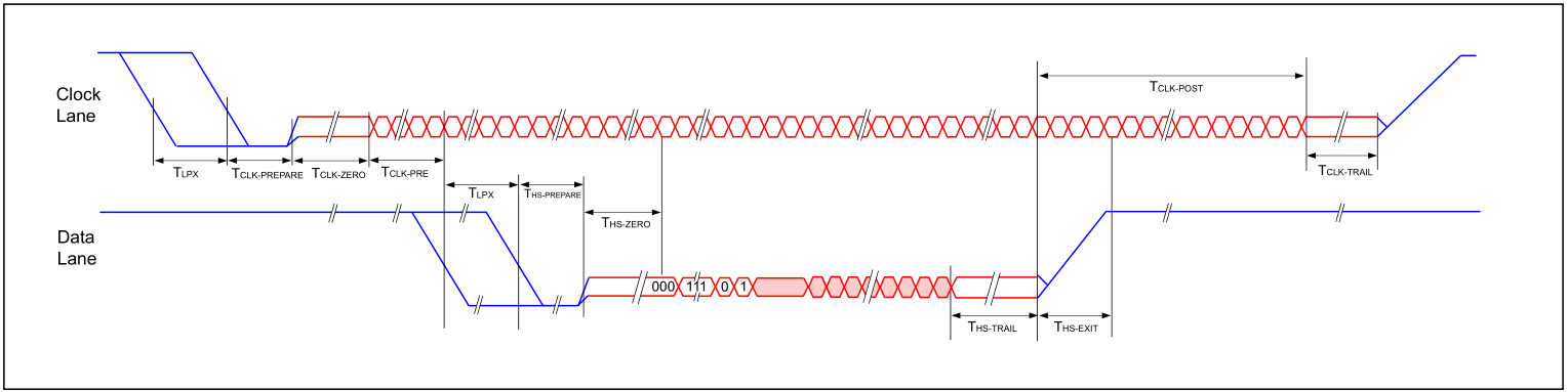
The MIPI DSI D-PHY configuration controls timing aspects of Low Power (LP) and High Speed (HS) communication. Configure these values to match specifications listed in the datasheet for the display.
Two internal channels may be used for command mode operations, available for all physical lane configurations. Channel-0 supports only LP mode (LP-TX, LP-RX), while Channel-1 supports LP mode (LP-TX, LP-RX) and HS mode (HS-TX).
There are two basic packet formats, short and long. Each format may be transmitted in high-speed or low-power modes. Packets may be followed by a Bus Turn-Around (BTA) request for reading information from the display. Once configured and started, video packets are transmitted automatically, until video output is stopped.
In addition to the full set of MIPI DSI commands, the application may trigger any of four special commands by setting flags in the message structure. These special commands are Reset Signal, Initial Skew Calibration, Periodic Skew Calibration, and No-Operation.
The application is notified of Acknowledge and Error Reporting (AwER) via an optional receive interrupt event. The most recent and accumulated AwER data may be retrieved by calling R_MIPI_DSI_StatusGet(). The application may send a MIPI_DSI_CMD_FLAG_BTA_NO_WRITE message with tx size of zero to request AwER from the peripheral.
Ultra-low Power State (ULPS) may be actived when HS and LP operations are not occurring. Clock and Data lanes may be transitioned into ULPS independently from each other.
Developers should be aware of the following limitations when using the MIPI DSI API:
When enabled, Interrupts will invoke the configured callback function. Low-power and High-Speed command status should be determined by checking Sequence 0 and Sequence 1 events, respectively. See the DSI Error Handling section of the user manual for information about how to handle error events.
Especially for use with display middleware such as emWin or GUIX, the callback will be invoked with post-open and pre-video-start events. Depending on your hardware, it may be necessary to use these events to configure the display.
This is a basic example showing the minimum code required to initialize and start the MIPI DSI module.
Data Structures | |
| struct | mipi_dsi_irq_cfg_t |
| struct | mipi_dsi_extended_cfg_t |
| struct | mipi_dsi_instance_ctrl_t |
| struct mipi_dsi_irq_cfg_t |
| struct mipi_dsi_extended_cfg_t |
Extended configuration structure for MIPI DSI.
| Data Fields | ||
|---|---|---|
| mipi_dsi_irq_cfg_t | dsi_seq0 | Sequence 0 interrupt. |
| mipi_dsi_irq_cfg_t | dsi_seq1 | Sequence 1 interrupt. |
| mipi_dsi_irq_cfg_t | dsi_ferr | DSI Fatal Error interrupt. |
| mipi_dsi_irq_cfg_t | dsi_ppi | D-PHY PPI interrupt. |
| mipi_dsi_irq_cfg_t | dsi_rcv | Receive interrupt. |
| mipi_dsi_irq_cfg_t | dsi_vin1 | Video Input Operation interrupt. |
| uint32_t | dsi_rxie | Receive interrupt enable configuration. |
| uint32_t | dsi_ferrie | Fatal error interrupt enable configuration. |
| uint32_t | dsi_plie | Physical lane interrupt enable configuration. |
| uint32_t | dsi_vmie | Video mode interrupt enable configuration. |
| uint32_t | dsi_sqch0ie | Sequence Channel 0 interrupt enable configuration. |
| uint32_t | dsi_sqch1ie | Sequence Channel 1 interrupt enable configuration. |
| struct mipi_dsi_instance_ctrl_t |
MIPI DSI instance control block.
Data Fields | |
| uint32_t | open |
| Interface is open. | |
| bool | data_ulps_active |
| Data lane ULPS status. | |
| bool | clock_ulps_active |
| Data lane ULPS status. | |
| mipi_dsi_lane_t | ulps_status |
| Ultra-low Power State active status. | |
| mipi_dsi_cfg_t const * | p_cfg |
| Pointer to configuration structure used to open the interface. | |
| void(* | p_callback )(mipi_dsi_callback_args_t *) |
| Pointer to callback that is called when an adc_event_t occurs. | |
| void * | p_context |
| Pointer to context to be passed into callback function. | |
| mipi_dsi_callback_args_t * | p_callback_memory |
| Pointer to non-secure memory that can be used to pass arguments to a callback in non-secure memory. | |
| fsp_err_t R_MIPI_DSI_Open | ( | mipi_dsi_ctrl_t *const | p_api_ctrl, |
| mipi_dsi_cfg_t const *const | p_cfg | ||
| ) |
Initialize the MIPI DSI peripheral.
| FSP_SUCCESS | The channel was successfully opened. |
| FSP_ERR_ASSERTION | One or both of the parameters was NULL. |
| FSP_ERR_ALREADY_OPEN | The instance is already opened. |
| FSP_ERR_INVALID_STATE | Display module must be opened before DSI. |
| fsp_err_t R_MIPI_DSI_Close | ( | mipi_dsi_ctrl_t *const | p_api_ctrl | ) |
Close MIPI DSI and display data instances, disable interrupts, and power-off the module.
| FSP_SUCCESS | The channel is successfully closed. |
| FSP_ERR_ASSERTION | p_api_ctrl is NULL. |
| FSP_ERR_NOT_OPEN | Instance is not open. |
| FSP_ERR_IN_USE | Operation in progress and must be stopped before closing. |
| fsp_err_t R_MIPI_DSI_Start | ( | mipi_dsi_ctrl_t *const | p_api_ctrl | ) |
Start video output. Initialize Video Output Registers Perform sequence steps 3 to 5 from "Start of Video Mode Operation" in the MIPI DSI section of the relevant hardware manual.
| FSP_SUCCESS | Data is successfully written to the D/A Converter. |
| FSP_ERR_ASSERTION | p_api_ctrl is NULL. |
| FSP_ERR_NOT_OPEN | Instance is not open. |
| FSP_ERR_IN_USE | The physical interface is currently in use. |
| FSP_ERR_INVALID_STATE | DSI is already in video mode. |
| fsp_err_t R_MIPI_DSI_Stop | ( | mipi_dsi_ctrl_t *const | p_api_ctrl | ) |
Stop video output.
| FSP_SUCCESS | Data is successfully written to the D/A Converter. |
| FSP_ERR_ASSERTION | p_api_ctrl is NULL. |
| FSP_ERR_NOT_OPEN | Instance is not open. |
| FSP_ERR_IN_USE | DSI cannot be closed while ULPS is active. |
| fsp_err_t R_MIPI_DSI_UlpsEnter | ( | mipi_dsi_ctrl_t *const | p_api_ctrl, |
| mipi_dsi_lane_t | lane | ||
| ) |
Enter Ultra-low Power State (ULPS).
| FSP_SUCCESS | Information read successfully. |
| FSP_ERR_ASSERTION | p_api_ctrl is NULL. |
| FSP_ERR_NOT_OPEN | Instance is not open. |
| FSP_ERR_INVALID_MODE | Invalid mode for transition. |
| fsp_err_t R_MIPI_DSI_UlpsExit | ( | mipi_dsi_ctrl_t *const | p_api_ctrl, |
| mipi_dsi_lane_t | lane | ||
| ) |
Exit Ultra-low Power State (ULPS).
| FSP_SUCCESS | Information read successfully. |
| FSP_ERR_ASSERTION | p_api_ctrl is NULL. |
| FSP_ERR_NOT_OPEN | Instance is not open. |
| fsp_err_t R_MIPI_DSI_Command | ( | mipi_dsi_ctrl_t *const | p_api_ctrl, |
| mipi_dsi_cmd_t * | p_cmd | ||
| ) |
Send a command to the peripheral device.
| FSP_SUCCESS | Command(s) queued successfully. |
| FSP_ERR_ASSERTION | p_api_ctrl is NULL. cmd_id specifies a long packet but p_data is NULL. |
| FSP_ERR_NOT_OPEN | Instance is not open. |
| FSP_ERR_IN_USE | The physical interface is currently in use or video mode is in operation. |
| FSP_ERR_INVALID_POINTER | Invalid pointer provided |
| FSP_ERR_INVALID_ARGUMENT | Invalid message configuration |
| fsp_err_t R_MIPI_DSI_StatusGet | ( | mipi_dsi_ctrl_t *const | p_api_ctrl, |
| mipi_dsi_status_t * | p_status | ||
| ) |
Provide information about current MIPI DSI status.
Note: Accumulated Acknowledge and Error (AwER) Status is cleared by calling this function. Latest AwER status is only set upon reception from peripheral.
| FSP_SUCCESS | Information read successfully. |
| FSP_ERR_ASSERTION | p_api_ctrl is NULL. |
| FSP_ERR_NOT_OPEN | Instance is not open. |